· AtlasPCB Engineering · Engineering · 11 min read
PCB DFM Check for High-Speed Designs: Signal Integrity Constraints Your Manufacturer Must Verify
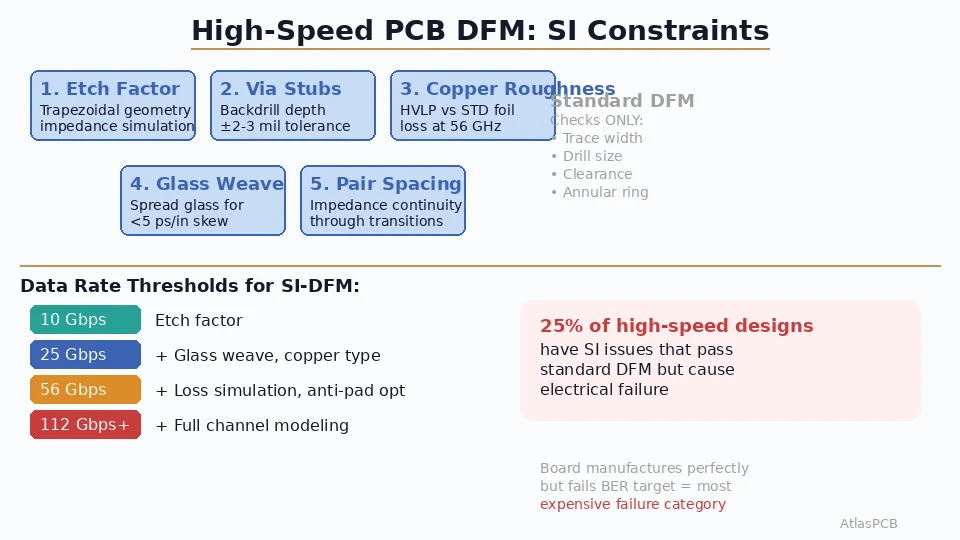
Standard DFM checks miss the critical signal integrity constraints that cause high-speed board failures. This guide covers the DFM verification points specific to 10+ Gbps designs — impedance-critical geometry, via stub management, loss budget validation, and the fabrication tolerances that determine whether your board actually works at speed.
Quick Answer
Standard PCB DFM checks verify manufacturing producibility (trace width, drill size, clearance) but miss the signal integrity constraints that determine whether a high-speed board functions at data rate. For designs running 10+ Gbps, your manufacturer must additionally verify: impedance-sensitive geometry including etch factor compensation, via stub length versus frequency-dependent loss budget, differential pair spacing consistency through routing transitions, and copper roughness impact on insertion loss. These SI-specific DFM checks prevent the most expensive category of PCB failure — boards that manufacture perfectly but fail electrically.
The Problem: Your Board Manufactures Perfectly But Fails at Speed
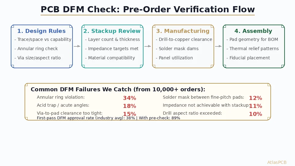
Standard PCB DFM checking verifies whether a board can be physically manufactured: minimum trace widths achievable with your fabricator’s etching process, drill sizes within their mechanical capability, clearances meeting voltage requirements, and annular rings large enough to survive registration tolerance. These checks ensure your board comes back as a physical object — but they tell you nothing about whether it will actually pass your 56 Gbps PAM4 bit error rate target.
The most expensive category of PCB failure in high-speed design is the board that passes all standard DFM checks, manufactures without defect, arrives on time, gets assembled perfectly — and then fails eye diagram measurements. You have spent NRE tooling, assembly cost, and 3-4 weeks of lead time to discover that your fabricator’s standard etch process created 3 ohms of impedance error on a critical net, or that the via stub residual after backdrilling is 8 mils instead of the 4 mils your loss budget assumed.
High-speed DFM review bridges this gap. It verifies not just “can we build this?” but “will it work at your target data rate given our specific fabrication process parameters?” This requires the manufacturer to understand your electrical requirements, not just your geometry. In our engineering review process, approximately 25% of high-speed designs we receive have at least one issue that would pass standard DFM but cause electrical failure.
HIGH-SPEED DFM REVIEW
Signal Integrity DFM Included with Every High-Speed Quote
Upload your Gerber + stackup. Our SI engineers verify impedance geometry, via stubs, loss budget, and copper roughness impact before production.
Upload for DFM Review ›DFM Check 1: Etch Factor and Impedance Geometry
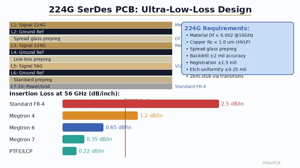
Every subtractive etch process creates trapezoidal copper traces. The etch factor — ratio of copper thickness to undercut — varies from 2.0 (aggressive) to 4.0 (controlled) depending on your fabricator’s etch chemistry, conveyor speed, and copper weight. A trace designed at 4.0 mil width in your EDA tool will not be 4.0 mil on the finished board. On 1oz copper (1.4 mil thick), typical undercutting produces a trace that is 4.0 mil at the base and 2.8-3.2 mil at the top, with an average width of approximately 3.5 mil.
Your impedance calculation should use the trapezoidal cross-section, not the rectangular CAD dimension. Most EDA field solvers default to rectangular geometry unless explicitly configured otherwise. If your designer calculates 50 ohms assuming rectangular 4.0 mil trace and your fabricator delivers trapezoidal 3.5 mil average width, the manufactured impedance will be 52-54 ohms — possibly outside your ±5% tolerance from this single factor alone.
What to verify in DFM review: Ask your fabricator what etch factor their process achieves on your specific copper weight and layer construction (inner vs outer layers etch differently due to different etch equipment). Confirm their impedance simulation uses trapezoidal geometry with their actual etch factor, not textbook rectangles. For inner layers on 0.5oz copper, etch factor is typically better (3.0-4.0) than outer layers on 1oz copper (2.0-3.0) because thinner copper requires less etch time and thus less lateral undercut.
At our facility, we characterize etch factor monthly for each copper weight and update our impedance simulation parameters accordingly. Our field solver models include measured etch factors that correlate to within ±0.5 ohm of actual TDR measurements on production panels — significantly better than the ±2-3 ohm error common when using nominal trace widths with rectangular assumptions.
DFM Check 2: Via Stub Length and Backdrill Depth Control
Via stubs create quarter-wave resonant notches in your channel frequency response. The first resonant null occurs at f = 7500/L (GHz, with L in mils). For a through-via in a 93-mil thick 10-layer board with signal on Layer 2, the stub length from Layer 2 to the board bottom is approximately 78 mils — creating a resonant notch at 96 GHz. For 25 Gbps NRZ (12.5 GHz fundamental), this stub seems safe. But the stub also creates distributed capacitance and frequency-dependent loss that degrades the channel well below the resonant frequency.
Practical stub length limits based on our production experience and customer feedback:
| Data Rate | Maximum Stub Length | Backdrill Depth Tolerance Needed |
|---|---|---|
| 10 Gbps NRZ | 25-30 mils | ±5 mil (standard) |
| 25 Gbps NRZ | 10-12 mils | ±4 mil |
| 56 Gbps PAM4 | 5-6 mils | ±3 mil (premium) |
| 112 Gbps PAM4 | 3-4 mils | ±2 mil (advanced) |
| 224 Gbps PAM4 | Not viable — use blind/buried vias | N/A |
What DFM must verify: Your fabricator’s actual backdrill depth accuracy, not their catalog specification. Many shops claim ±4 mil tolerance but achieve ±6-7 mil in practice on complex boards with multiple drill hits. Ask for their backdrill cpk data from recent production. If your design requires ±3 mil, confirm their equipment and process can deliver this consistently — some manufacturers achieve it only with x-ray measurement feedback systems.
In our production line, we achieve ±3 mil backdrill depth accuracy using automated depth control with impedance-sensing drill spindles. For designs requiring better than ±3 mil, we recommend blind/buried via construction to eliminate stubs entirely rather than pushing backdrill tolerance beyond reliable process capability.
PRECISION BACKDRILLING
±3 mil Backdrill Depth Accuracy — Verified on Every Panel
Impedance-sensing drill control with cross-section verification. Supporting 56G PAM4 and 112G designs with consistent stub management.
View Capabilities ›DFM Check 3: Copper Roughness Impact on Insertion Loss
Copper foil roughness is the single largest source of additional insertion loss at frequencies above 5 GHz, yet most standard DFM reviews completely ignore it. The mechanism is well understood: current at high frequencies concentrates in the skin depth layer (approximately 0.66 um at 10 GHz in copper). If the copper surface roughness Rz exceeds the skin depth, the effective conductor path length increases dramatically — current must travel over and around the rough peaks rather than flowing along a smooth surface.
The impact quantified from our production measurements on identical impedance structures:
| Copper Type | Rz (um) | Additional Loss at 10 GHz | Additional Loss at 28 GHz |
|---|---|---|---|
| Standard electrodeposited (STD) | 5-8 | +0.15 dB/inch | +0.35 dB/inch |
| Reverse-treated foil (RTF) | 3-5 | +0.08 dB/inch | +0.20 dB/inch |
| Very-low-profile (VLP) | 1.5-3 | +0.04 dB/inch | +0.12 dB/inch |
| Hyper-VLP (HVLP) | 0.8-1.5 | +0.02 dB/inch | +0.06 dB/inch |
For a 6-inch differential pair channel at 28 GHz, the difference between STD and HVLP copper is 1.7 dB of additional loss — often enough to push a marginally passing channel into failure. Yet standard DFM review only verifies copper weight (1oz, 0.5oz), not copper type.
What DFM must verify: Confirm your fabricator stocks and processes the copper foil type your loss simulation assumes. If you designed assuming VLP copper and your fabricator substitutes RTF (common when shops run low on specialty foils), your channel loses 0.5-1.0 dB of margin per 6 inches. This substitution is invisible to standard DFM checking and only appears when you measure insertion loss on the finished board.
DFM Check 4: Glass Weave Skew on Differential Pairs
Fiberglass reinforcement in FR-4 and most PCB laminates uses a woven structure with distinct glass and resin regions. The dielectric constant of glass (approximately 6.1) differs significantly from the surrounding resin (approximately 3.2). When differential pair traces happen to route parallel to the glass weave with one trace over glass and the other over resin, the effective Dk difference creates propagation velocity mismatch between the pair — intra-pair skew.
This effect is most severe on 1080 and 2116 glass styles where the weave window (resin-only region between glass bundles) is large enough that a 4-5 mil trace can sit entirely in resin while its pair partner rides on glass. The resulting skew can reach 5-10 ps/inch on these open-weave styles, which becomes problematic above 25 Gbps where total intra-pair skew budgets are often under 15 ps for 6-inch channels.
The DFM solution: For designs at 25 Gbps and above, specify spread-glass or flat-glass (NE-glass) prepreg where the weave structure is mechanically opened to reduce glass-resin periodicity. Alternatively, specify 1035 or 1078 glass styles where the tight weave pitch makes the effective Dk more uniform across the surface. Your DFM review should verify that your fabricator’s standard stackup uses glass styles appropriate for your data rate — many standard stackups default to 2116 glass in thick prepreg layers because it is cheaper and readily available.
At AtlasPCB, our standard high-speed stackups use 1078 spread glass on signal-adjacent prepreg layers for designs targeting 25+ Gbps. We flag any design at these data rates that arrives with unspecified glass style, because our default stackup choice directly affects glass weave skew performance.
ENGINEERED FOR HIGH SPEED
Stackups Optimized for 56G and 112G PAM4
Spread glass, HVLP copper, and precision backdrill as standard for high-speed designs. No hidden material substitutions.
Get High-Speed Quote ›DFM Check 5: Differential Pair Spacing Consistency Through Transitions
Maintaining consistent differential pair coupling through routing transitions — BGA breakout fans, via transitions between layers, and connector footprint entries — is critical for impedance continuity. A differential pair designed for 100-ohm impedance at 5/5 mil spacing suddenly becomes 110+ ohms when the pair separates to 12 mil spacing for via breakout, then returns to 100 ohms on the next layer.
Standard DFM checks verify minimum spacing but do not flag impedance-discontinuity regions. A pair that spreads from 5 mil to 15 mil gap for BGA escape passes minimum spacing checks but creates a localized impedance spike that degrades return loss by 3-6 dB at high frequencies. At 56 Gbps PAM4, this single impedance discontinuity in the via breakout can reduce timing margin by 5-10% — enough to shift a passing channel to marginal.
What DFM should verify: Identify all locations where impedance-critical differential pairs change spacing by more than 2x their nominal gap, and flag these as impedance discontinuity points. The fabricator should confirm that their etch compensation is appropriate at both the nominal and spread-out spacing (wider gap = less etch loading = different effective trace width). For anti-pad clearances in ground planes at via transitions, verify that the reference plane gap does not exceed 2x the trace-to-reference distance.
Your High-Speed DFM Checklist
Before sending your high-speed design (10+ Gbps) to a fabricator, verify they address these signal integrity DFM points:
| DFM Verification Point | Data Rate Threshold | What to Ask Your Fabricator |
|---|---|---|
| Trapezoidal impedance simulation | All impedance-controlled | ”Do you use measured etch factors in your impedance model?” |
| Backdrill depth tolerance | 25 Gbps+ | “What is your cpk on backdrill depth? Provide recent data.” |
| Copper roughness specification | 10 Gbps+ | “Which copper foil type do you use? Can you guarantee HVLP?” |
| Glass weave style on signal layers | 25 Gbps+ | “What glass style is on prepreg adjacent to my signal layers?” |
| Differential pair transition analysis | 25 Gbps+ | “Do you flag impedance discontinuity regions in DFM?” |
| Loss budget simulation | 56 Gbps+ | “Can you simulate total channel loss with your materials/process?” |
| Anti-pad optimization | 25 Gbps+ | “Do you optimize via anti-pad for impedance matching?” |
| Surface finish loss impact | 56 Gbps+ | “What is the measured additional loss from your ENIG process?” |
If your fabricator cannot answer these questions with specific data from their process, they are not equipped to reliably produce boards for your data rate target. A board that manufactures but fails electrically is more expensive than one that never gets built — it consumes assembly cost, component cost, and weeks of debug time.
ATLASPCB
High-Speed DFM That Goes Beyond Manufacturing Checks
Our SI-aware DFM review catches the signal integrity issues standard checks miss. Every high-speed design gets etch factor analysis, loss budget estimation, and material verification before first article.
Submit Design for Review ›Reviewed by AtlasPCB Engineering Team — 15+ years in advanced PCB fabrication for RF, HDI, and rigid-flex applications.
Related Reading:
About AtlasPCB — We specialize in complex PCB manufacturing for HDI, RF, and high-reliability applications. Explore our HDI PCB manufacturing capabilities, RF and high-frequency PCB services, or get an impedance-controlled PCB manufacturing . Every order includes free engineering review. Get your quote.
Reviewed by AtlasPCB Engineering Team — IPC-certified manufacturing specialists with 15+ years of production experience in HDI, RF, and high-reliability PCB fabrication. Content based on factory floor data and real customer design reviews.
Frequently Asked Questions
What DFM checks are specific to high-speed PCB designs?
At what data rate should I request high-speed DFM review?
How does etch factor affect high-speed signal integrity?
What is the relationship between via stub length and maximum data rate?
Should I ask my PCB manufacturer for a loss budget simulation?
- PCB DFM check
- impedance controlled PCB manufacturer
- PCB stackup design guide
- RF PCB design and manufacturing
- HDI PCB manufacturer