· AtlasPCB Engineering · Engineering · 11 min read
5G mmWave Phased Array PCB: Rogers 4350B Stackup Design for 28/39 GHz Antenna Modules
Building a 28 or 39 GHz phased array antenna module demands PCB specifications that push beyond standard RF fabrication. This guide covers the specific stackup architecture, material constraints, and manufacturing tolerances required for mmWave antenna array feed networks — with validated Rogers 4350B configurations from production builds.
Quick Answer
A 28/39 GHz phased array antenna PCB requires a hybrid stackup: Rogers RO4350B (Dk 3.48, Df 0.0037) for the antenna radiating layer and feed network, combined with standard FR-4 or Megtron for digital beamforming control layers. Critical manufacturing requirements include ±0.5 mil dielectric thickness tolerance on the antenna layer, copper surface roughness below 1.5 um RMS (rolled annealed foil preferred), and etch tolerance under ±0.3 mil for patch antenna dimensions. Standard PCB shops cannot fabricate mmWave antenna arrays — this requires RF-specialized facilities with material characterization at operating frequency.
The 30-Second Decision
| Parameter | mmWave Antenna PCB | Standard RF PCB | Why It Matters at 28 GHz |
|---|---|---|---|
| Dielectric tolerance | ±0.5 mil | ±1.0 mil | ±1 mil = ±400 MHz freq shift |
| Copper roughness | Under 1.5 um RMS | Under 3 um RMS | Roughness adds 0.3-0.8 dB/inch at 28 GHz |
| Etch tolerance | ±0.3 mil (7.5 um) | ±0.5 mil (12.5 um) | Patch width error = antenna mismatch |
| Material Dk stability | ±1% over temp | ±3% acceptable | Array phase coherence depends on Dk match |
| Registration (layer-to-layer) | ±1 mil | ±2 mil | Feed-to-antenna alignment critical |
Why 28/39 GHz Changes Everything About PCB Fabrication
Designing a PCB antenna array at 28 GHz means operating where the free-space wavelength is 10.7mm — and the guided wavelength on RO4350B substrate is approximately 5.7mm. A standard patch antenna element at this frequency measures roughly 2.8mm x 2.8mm. At these dimensions, fabrication tolerances that are irrelevant at lower frequencies become dominant error sources.
Consider the math: a ±0.3 mil (7.5 um) etch tolerance on a 2.8mm-wide patch represents approximately ±0.3% dimensional accuracy. At 2.4 GHz (where the same patch would be 38mm wide), that same ±0.3 mil tolerance is ±0.02% — essentially perfect. This dimensional sensitivity is why mmWave antenna PCB fabrication is fundamentally different from sub-6 GHz RF board work.
The second critical difference is copper surface roughness. Standard electrodeposited (ED) copper foil has surface roughness of 2-5 um RMS. At 2.4 GHz, skin depth is approximately 1.3 um — meaning current flows deep enough that surface roughness has minimal impact. At 28 GHz, skin depth drops to 0.4 um. The current is confined to a layer thinner than the surface roughness features, dramatically increasing conductor loss. For mmWave antenna feed networks where we’ve measured production boards side-by-side, switching from standard ED foil (3 um RMS) to rolled-annealed (RA) foil (0.8 um RMS) reduces feed network loss by 0.3-0.5 dB per inch at 28 GHz — a massive improvement when feed networks run 20-40mm long.
MMWAVE PCB SPECIALIST
Rogers 4350B Processing with Verified mmWave Performance
We characterize material Dk at your operating frequency, specify low-roughness copper, and verify antenna dimensions with optical measurement. Not just an RF board — a validated antenna.
RF PCB Services ›
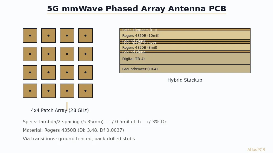
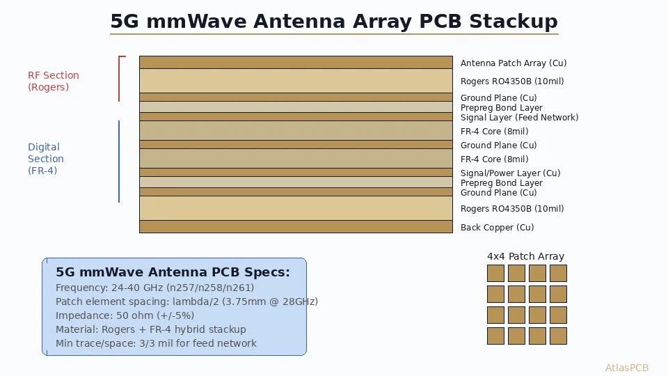
Validated Stackup Architecture for 28 GHz 16-Element Array
Based on production builds we’ve delivered for 5G small cell and fixed wireless access (FWA) applications, the following hybrid Rogers/FR-4 stackup provides proven performance at 28 GHz with manageable fabrication complexity.
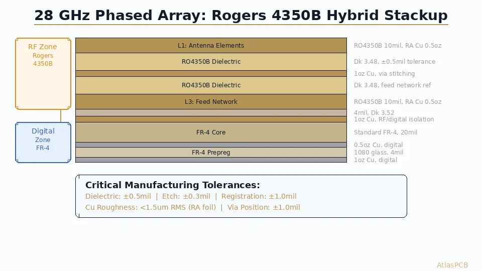
The 6-layer architecture separates the design into three functional zones. The top two Rogers layers handle all mmWave radiation and feed distribution — this is where fabrication precision matters most. The bottom two FR-4 layers carry DC bias networks for the beamforming IC (phase shifters, LNAs, PAs) and digital control signals. This separation means the expensive, tight-tolerance Rogers processing applies only to the layers that need it, while standard FR-4 fabrication handles everything else.
Layer 1 — Antenna Elements (RO4350B, 10 mil, RA copper 0.5oz): Patch antenna array with corporate or series feed points. Copper surface roughness specified at 1.2 um RMS maximum (rolled-annealed foil). Etch tolerance ±0.3 mil per element edge. Antenna dimensions verified with automated optical measurement post-etch.
Layer 2 — Ground Plane (1oz ED copper): Continuous ground reference for antenna elements. Via stitching at lambda/20 spacing (0.5mm pitch at 28 GHz) around array periphery to suppress surface wave propagation and maintain element isolation.
Layer 3 — Feed Network (RO4350B, 10 mil, RA copper 0.5oz): Corporate feed network (Wilkinson dividers, quarter-wave transformers) distributing signal to each antenna element. Characteristic impedance 50 ohm ±3%. Phase-matched trace lengths to maintain beam pointing accuracy.
Layer 4 — Ground Plane (1oz ED copper): Provides isolation between RF and digital sections. Solid plane with minimal apertures — only via clearances for interlayer connections.
Bondply (RO4450F, 4 mil): Rogers-to-FR-4 transition layer. RO4450F chosen for compatible lamination temperature with both Rogers and FR-4, and Dk of 3.52 that doesn’t create significant impedance discontinuity at the transition.
Layer 5 — DC Bias/Control (FR-4, 6 mil, 0.5oz): DC power distribution for RFIC, LNA bias, phase shifter control voltages. Standard FR-4 adequate — no RF signals on this layer.
Layer 6 — Digital/Ground (FR-4, 1oz): SPI/I2C control for beamforming IC, power regulation, connector footprints. Standard fabrication tolerance acceptable.
Total stackup thickness: approximately 62 mil (1.57mm). This fits within standard SMT assembly equipment constraints while providing adequate mechanical rigidity for a 50x50mm antenna module.
Manufacturing Tolerances That Make or Break mmWave Arrays
Phased array performance depends on element-to-element consistency — both in amplitude and phase. At 28 GHz, manufacturing variations that are invisible at lower frequencies create measurable beam degradation.
Dielectric Thickness Variation: The antenna element resonant frequency scales inversely with the square root of substrate thickness. For a 10-mil RO4350B substrate at 28 GHz: every 0.1 mil thickness variation shifts resonant frequency by approximately 40 MHz. The 28 GHz n257 band spans 26.5-29.5 GHz, but a typical antenna element has 3-5% bandwidth (approximately 1-1.4 GHz). A ±1 mil dielectric variation across the panel would produce ±400 MHz resonance spread across elements — potentially pushing edge elements outside the operating band.
We specify ±0.5 mil tolerance on the antenna dielectric layer, verified by micrometer measurement at 5 points per panel. Rogers material incoming inspection confirms thickness uniformity before processing. This tolerance level maintains element resonance spread within ±200 MHz — keeping all elements operational across the target band with margin for temperature variation.
Phase Error from Feed Network: In a corporate feed network distributing signal to 16 elements, trace length matching must maintain phase error below ±5 degrees at 28 GHz for acceptable beam pointing. At lambda = 5.7mm in the substrate, ±5 degrees corresponds to ±0.08mm (3.1 mil) trace length accuracy. This is achievable with standard CNC routing and etch process control, but requires the manufacturer to understand that feed trace length tolerance is tighter than typical digital routing (where ±5 mil is routine).
Element Amplitude Balance: The Wilkinson divider network should deliver equal amplitude to all elements within ±0.5 dB. The primary error source is conductor loss variation from copper roughness non-uniformity across the panel. Using rolled-annealed foil with verified roughness under 1.5 um RMS limits amplitude variation to under ±0.3 dB across 16 elements based on our production measurements.
PRECISION RF FABRICATION
±0.5 mil Dielectric Tolerance on Rogers 4350B — Verified Per Panel
Not just "we process Rogers" — we characterize, measure, and verify every critical dimension for mmWave antenna performance. Your beam patterns depend on our tolerances.
Get mmWave PCB Quote ›Via Transitions and Vertical Interconnects at 28 GHz
Connecting the antenna layer to the feed network through a ground plane requires via transitions that maintain 50-ohm impedance through the vertical path. At 28 GHz, standard PTH vias (0.2-0.3mm drill) behave as short transmission line segments with significant parasitic inductance and capacitance.
The proven approach for mmWave via transitions uses ground-signal-ground (GSG) via arrays — one signal via surrounded by 4-6 ground vias at radius of 0.3-0.5mm. The ground vias create a coaxial-like structure that maintains impedance control through the layer transition. In our production, we achieve better than -15 dB return loss on via transitions at 28 GHz using 0.2mm signal vias with 0.15mm clearance annulus and 4 ground vias at 0.4mm radius — all achievable with mechanical drilling.
For antenna feed connections specifically, the via from Layer 3 (feed network) through Layer 2 (ground plane) to Layer 1 (antenna element) requires a clearance hole in the ground plane. This aperture must be sized carefully: too small creates excessive capacitance (lowering impedance), too large allows feed radiation (increasing coupling between elements). A clearance diameter of 0.6-0.8mm (lambda/10 to lambda/7 at 28 GHz) provides good compromise, verified by full-wave simulation.
One manufacturing consideration often overlooked: the back-drill depth accuracy for removing via stubs below the feed layer. A via stub extending 10-20 mil below Layer 3 creates a resonant structure at 28 GHz that can radiate or absorb energy depending on stub length. We offer backdrilling with ±3 mil depth accuracy, which limits residual stub to under 5 mil — keeping stub resonance well above the operating band.
Material Procurement and Lead Time Reality for mmWave Arrays
Rogers RO4350B in the specific configurations required for mmWave antenna PCBs (10 mil with RA copper) is not a stock item for most PCB manufacturers. The material supply chain adds significant lead time that hardware teams must account for in their development schedule.
Standard RO4350B with ED copper (the most common configuration for sub-10 GHz designs) is typically available from Rogers distributors within 2-3 weeks. However, the low-roughness RA copper variant adds 4-6 weeks because it’s produced in smaller quantities and often requires minimum order sizes (5-10 panels). The RO4450F bondply for hybrid lamination adds another potential bottleneck — this is a specialty prepreg used primarily for Rogers-to-Rogers or Rogers-to-FR-4 bonding.
At our facility, we maintain buffer stock of RO4350B 10-mil in both ED and RA copper variants due to consistent demand from 5G antenna customers. This typically saves 3-4 weeks versus ordering from Rogers distribution. However, exotic thicknesses (5 mil, 20 mil, 30 mil) or non-standard copper weights require lead time planning.
For teams developing 5G mmWave antenna modules, we recommend engaging with your PCB manufacturer during the simulation phase — before PCB layout is complete. This allows material procurement to run in parallel with design finalization, compressing the overall schedule by 4-6 weeks. We’ve had customers achieve first prototype delivery within 4 weeks of layout completion by pre-ordering material during simulation validation.
CHINA RF PCB MANUFACTURER
Rogers 4350B in Stock — mmWave Builds Ship in 3-4 Weeks
We stock common Rogers configurations for 5G antenna applications. Pre-order material during your design phase to avoid 6-week material lead time delays.
Design Rules Summary for 28/39 GHz Phased Array PCBs
For hardware engineers beginning a mmWave phased array design, these fabrication-constrained design rules represent achievable specifications at our facility without extraordinary processing:
| Parameter | 28 GHz Specification | 39 GHz Specification | Fabrication Method |
|---|---|---|---|
| Min patch dimension tolerance | ±0.3 mil (7.5 um) | ±0.2 mil (5 um) | Laser direct imaging + controlled etch |
| Dielectric thickness tolerance | ±0.5 mil | ±0.3 mil | Pre-measured material, controlled layup |
| Copper roughness (RA) | Under 1.5 um RMS | Under 1.0 um RMS | Rolled-annealed foil specification |
| Feed trace impedance | 50 ohm ±3% | 50 ohm ±3% | Field-solver stackup, TDR verified |
| Layer registration | ±1.0 mil | ±0.75 mil | X-ray alignment, optical targets |
| Via position accuracy | ±1.0 mil | ±0.75 mil | CNC drill with optical datum |
| Min trace/space on antenna layer | 3/3 mil (75 um) | 3/3 mil (75 um) | LDI exposure, spray etch |
| Backdrilling depth accuracy | ±3 mil | ±2 mil | Controlled-depth drilling with X-ray |
The 39 GHz column represents tighter specifications that increase cost by approximately 20-30% over 28 GHz builds due to higher reject rates. Most development programs start at 28 GHz (larger dimensions, more forgiving tolerances) before scaling to 39 GHz.
ATLASPCB
Building a 5G mmWave Antenna? Let's Talk Stackup First
Send your array specifications and frequency band requirements. We'll provide a validated Rogers 4350B stackup and confirmed fabrication tolerances for your specific phased array design.
Start mmWave Project ›
Reviewed by AtlasPCB Engineering Team — 15+ years in advanced PCB fabrication for RF, HDI, and rigid-flex applications.
Related Reading:
About AtlasPCB — We specialize in complex PCB manufacturing for HDI, RF, and high-reliability applications. Explore our RF and high-frequency PCB services, or get an multilayer PCB fabrication up to 30 layers . Every order includes free engineering review. Get your quote.
Reviewed by AtlasPCB Engineering Team — IPC-certified manufacturing specialists with 15+ years of production experience in HDI, RF, and high-reliability PCB fabrication. Content based on factory floor data and real customer design reviews.
Frequently Asked Questions
Why is Rogers 4350B preferred for 5G mmWave antenna arrays?
What stackup structure works for a 28 GHz 16-element phased array?
Can a standard PCB manufacturer build a 28 GHz phased array?
How much does a 5G mmWave phased array PCB cost?
What is the most common fabrication failure mode on mmWave antenna PCBs?
- 5G antenna PCB fabrication
- Rogers 4350B stackup
- RF PCB design and manufacturing
- China RF PCB manufacturer
- phased array
- mmWave