· Sophia Reyes · Engineering · 8 min read
Differential Pair Routing
Master differential pair routing with this engineering guide on tight vs loose coupling. Learn when to use each approach for USB, PCIe, DDR5, HDMI, and RF applications with impedance calculations and layout examples.
Quick Answer
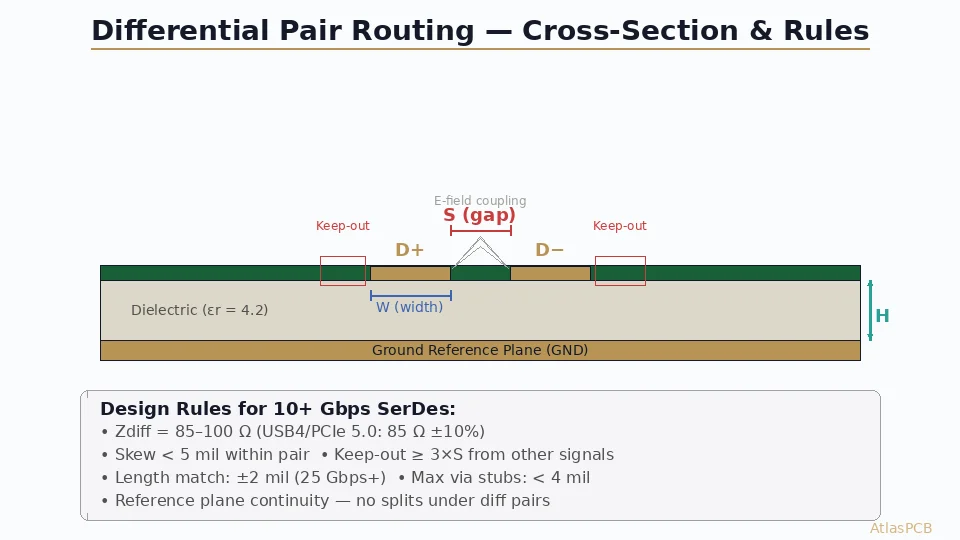
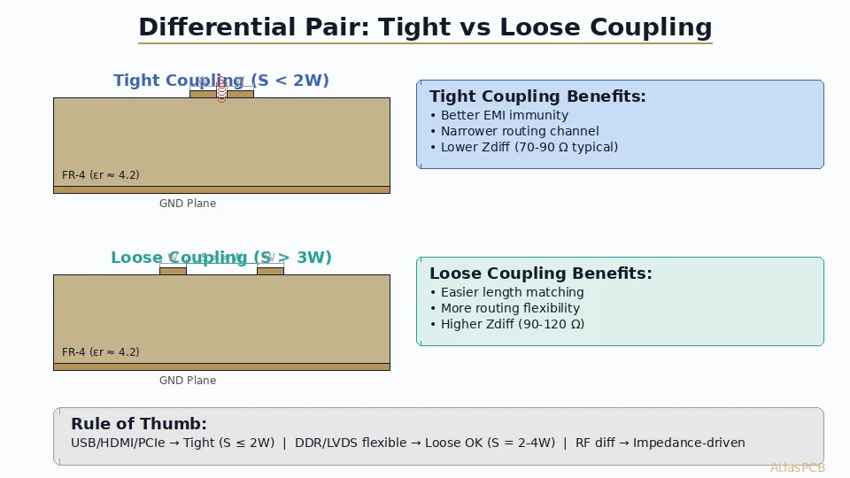
Tight coupling (spacing S ≤ 2× trace width W) provides better EMI immunity, narrower routing channels, and lower differential impedance (typically 85–100 Ω), making it ideal for USB, PCIe, HDMI, and other protocols with strict coupling requirements. Loose coupling (S > 3W) simplifies length matching, provides more routing flexibility around obstacles, and produces higher differential impedance—suitable for DDR interfaces and situations where traces must separate around vias or components. The critical rule: maintain consistent spacing throughout the pair's entire route. Changing coupling mid-route creates impedance discontinuities that degrade signal quality far more than choosing one coupling style over another.
Why Differential Signaling Dominates High-Speed Design
Every major high-speed interface used in modern electronics relies on differential signaling: USB, PCIe, HDMI, DisplayPort, Ethernet, SATA, DDR (clock pairs), LVDS, and MIPI. The reason is fundamental—differential pairs reject common-mode noise, enabling reliable communication at speeds where single-ended signaling would fail.
But designing differential pairs isn’t just about running two traces—the coupling between traces directly determines impedance, EMI performance, crosstalk immunity, and routing density. This guide provides the engineering framework for choosing between tight and loose coupling strategies.
Understanding Coupling in Differential Pairs
The Physics of Coupling
When two parallel traces carry equal and opposite currents, their electromagnetic fields interact. The degree of interaction depends on spacing:
- Tight coupling (S ≤ 2W): Strong mutual inductance and capacitance between traces. Fields concentrate between the pair, creating a “transmission line mode” between them.
- Loose coupling (S > 3W): Weak mutual interaction. Each trace primarily references the ground plane below, behaving more like two independent single-ended traces with inverted signals.
Impact on Impedance
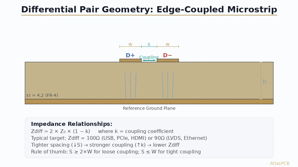
Differential impedance (Zdiff) relates to single-ended impedance (Z0) through coupling:
Zdiff = 2 × Z0 × (1 - k)Where k is the coupling coefficient (0 to 1):
- Tight coupling: k = 0.1 to 0.3 → Zdiff = 1.4×Z0 to 1.8×Z0
- Loose coupling: k ≈ 0 → Zdiff ≈ 2×Z0
This means tight coupling reduces differential impedance. To achieve the same 100 Ω Zdiff, tightly coupled traces need higher single-ended impedance (wider or thinner traces) compared to loosely coupled ones.
Tight Coupling: When and Why
Advantages
Superior EMI performance: Field confinement between traces reduces radiation. The equal-and-opposite currents create cancellation in the far field—but only when traces are close enough for effective cancellation.
Narrower routing channel: A 5-mil trace with 5-mil gap uses 15 mil total width vs 5-mil trace with 20-mil gap using 30 mil. Half the routing real estate.
Better common-mode rejection: External noise couples equally to both traces when they’re close together, maintaining the differential signal integrity.
Ground plane disruption tolerance: Tightly coupled pairs are less sensitive to reference plane voids because more energy travels between the traces rather than to the plane.
When to Use Tight Coupling
- USB 3.x/4: Specification mandates tight coupling for EMI compliance
- PCIe Gen 3/4/5: Intel/PCI-SIG design guides recommend S ≤ 2W
- HDMI 2.0/2.1: HDMI compliance testing measures coupling
- High-density BGA breakout: Space constraints require minimum pair width
- Backplane connectors: Dense differential pairs in connector fields
- Any EMI-sensitive design: FCC/CE compliance easier with tight coupling
Design Rules for Tight Coupling
Trace width (W): 4-5 mil typical (100 Ω differential)
Spacing (S): W to 2W (4-10 mil typical)
Reference plane distance: 3-5 mil (1080 or 2116 prepreg)
Minimum parallel length before coupling matters: >5× S
Keep consistent S throughout route: ±10% tolerance
Impedance-Controlled Manufacturing
±10% Impedance Tolerance, Verified with TDR
AtlasPCB provides impedance-controlled fabrication with coupon testing on every panel. Free stackup design assistance included.
Get Impedance Quote →Loose Coupling: When and Why
Advantages
Easier length matching: When traces separate around obstacles, there’s no coupling change—each trace independently references the ground plane.
Simpler routing around vias and pads: Traces can diverge without creating impedance steps. In tight coupling, any separation change creates a discontinuity.
Better manufacturing tolerance: Wider spacing is easier to etch consistently. At 4-mil space, a ±0.5 mil etch variation changes impedance by ~5%. At 12-mil space, the same variation changes impedance by <1%.
Lower crosstalk between adjacent pairs: More space between traces of the same pair means more space between adjacent pairs.
When to Use Loose Coupling
- DDR4/DDR5 data lines: JEDEC allows loose coupling; routing density more important
- LVDS interfaces: Often routed at S = 3-5W for manufacturing ease
- Long backplane traces: Where consistent tight spacing over 30+ cm is difficult
- BGA escape routing: Where traces must thread between via pads
- Designs with many layer transitions: Loose coupling is more forgiving at via transitions
- Budget PCBs: Wider spacing = looser manufacturing tolerance = lower cost
Design Rules for Loose Coupling
Trace width (W): 3.5-5 mil (adjust for target Zdiff)
Spacing (S): 3W to 5W (12-25 mil typical)
Reference plane: CRITICAL—must be continuous under both traces
Maximum length without matched ground: 0 mil (continuous reference required)
Pair-to-pair spacing: ≥3× intra-pair spacing
The Critical Rule: Consistency Over Choice
The most important differential pair rule isn’t tight vs loose—it’s maintaining consistent coupling throughout the route.
A 50-mil discontinuity in a tightly coupled pair (where S changes from 5 mil to 15 mil around a via pad) creates a localized impedance spike that reflects signal energy. This reflection can close the eye diagram margin more than choosing a suboptimal coupling strategy from the start.
How to Handle Unavoidable Spacing Changes
- Taper gradually: If spacing must change, do it over at least 5× the spacing difference (e.g., changing from 5 mil to 15 mil should taper over 50 mil minimum)
- Minimize transition length: Keep the non-uniform section as short as possible (<500 mil)
- Compensate with trace width: Some EDA tools can auto-adjust trace width as spacing changes to maintain constant Zdiff
- Add ground guard traces: Fill space with grounded copper to modify the effective impedance in the transition region
Protocol-Specific Recommendations
USB 3.2 / USB4 (5–40 Gbps)
| Parameter | Specification |
|---|---|
| Zdiff | 85 Ω ±15% (USB 3.x) or 85 Ω ±10% (USB4) |
| Coupling | Tight (S ≤ 2W recommended) |
| Intra-pair skew | ≤15 mil (USB 3.x), ≤6 mil (USB4) |
| Max trace length | 150 mm (USB 3.2 Gen 1) |
| Reference plane gaps | Prohibited under diff pair |
PCIe Gen 5 (32 GT/s)
| Parameter | Specification |
|---|---|
| Zdiff | 85 Ω ±10% |
| Coupling | Tight preferred |
| Intra-pair skew | ≤5 mil |
| Inter-pair skew | Per protocol lane group |
| Pair-to-pair spacing | ≥5× intra-pair S |
| Max via stubs | <6 mil (back-drill required) |
DDR5 (4800–8400 MT/s)
| Parameter | Specification |
|---|---|
| Zdiff (clock) | 80–100 Ω ±10% |
| Zdiff (DQS) | 80–100 Ω ±10% |
| Coupling | Moderate (S = 2-3W acceptable) |
| Clock intra-pair skew | ≤2 mil |
| DQS intra-pair skew | ≤5 mil |
| Note | DQ lines are single-ended, not differential |
HDMI 2.1 (48 Gbps)
| Parameter | Specification |
|---|---|
| Zdiff | 100 Ω ±10% |
| Coupling | Tight (S = W, 1:1 ratio) |
| Intra-pair skew | ≤5 mil within each channel |
| Inter-pair skew | ≤5 mil between all 4 channels |
| Maximum length | 100 mm (PCB trace, not cable) |
Impedance Calculation: Practical Examples
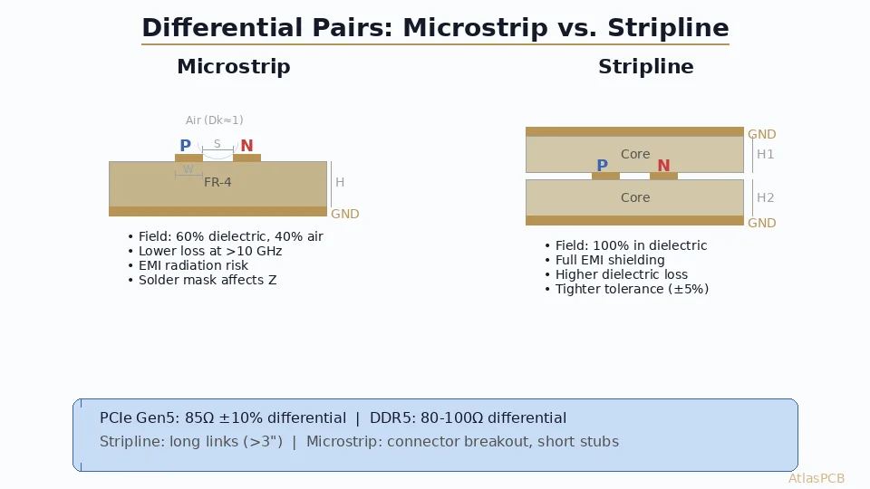
Example 1: Tight Coupled Microstrip, 100 Ω Zdiff
Stackup: 4-layer, 1080 prepreg (3.5 mil, Dk=4.2)
Copper: 1 oz (1.35 mil finished), rough profile
Target: 100 Ω differential

Solution (field solver):
  W = 4.5 mil
  S = 5.0 mil
  H = 3.5 mil to reference plane
  Zdiff = 99.4 Ω
  Z0 (odd) = 49.7 Ω
  k = 0.12
Example 2: Loose Coupled Stripline, 100 Ω Zdiff
Stackup: 6-layer, inner layer between two planes
Dielectric: 4.0 mil each side (Dk=4.0 @ 1 GHz)
Copper: 0.5 oz (0.7 mil)
Target: 100 Ω differential

Solution (field solver):
  W = 3.8 mil
  S = 15 mil
  H1 = H2 = 4.0 mil (centered stripline)
  Zdiff = 100.2 Ω
  Z0 (odd) ≈ Z0 (even) ≈ 50 Ω
  k = 0.02 (essentially uncoupled)
Common Routing Mistakes
Mistake 1: Breaking Coupling at BGA Escape
When routing from BGA pads, traces must fan out through the via field. A tightly coupled pair that suddenly separates to pass between vias creates a major discontinuity.
Solution: Commit to loose coupling for BGA escape areas, then taper to tight coupling in the open routing channel. Or use neck-down routing where both W and S reduce proportionally.
Mistake 2: Reference Plane Splits Under Diff Pairs
A split in the reference plane under a differential pair forces return current to detour, adding inductance and destroying impedance control.
Solution: Never route differential pairs across plane splits. If unavoidable, add stitching capacitors (100 nF) directly at the crossing point.
Mistake 3: Asymmetric Via Transitions
When a differential pair changes layers, both vias must be identical (same pad size, antipad, and back-drill). A non-symmetric transition converts differential signal energy to common-mode, which radiates.
Solution: Use paired vias with identical geometry. Add return-path stitching vias within 50 mil of the signal vias.
Mistake 4: Excessive Length Matching Serpentines
Adding large serpentines to match length introduces coupling between serpentine segments that distorts the signal.
Solution: Keep serpentine amplitude ≤3× trace width. Use gradual curves instead of sharp 90° bends. Place serpentines in the shorter trace only, not both.
Manufacturing Considerations
Etching and Spacing
Minimum production spacing varies by fabricator:
- Standard: 4 mil minimum (reliable at most shops)
- Advanced: 3 mil minimum (requires good process control)
- HDI: 2.5 mil (laser-direct-imaging required)
For impedance consistency, specify spacing at least 1 mil above your fabricator’s minimum. At the process edge, etch variation has maximum impact on impedance.
Impedance Testing
Request impedance coupon testing per IPC-TM-650 2.5.5.7:
- TDR (Time Domain Reflectometry) measurement
- Report format: impedance profile along trace length
- Acceptance: ±10% of target (or ±5% for Thunderbolt/USB4)
- Test coupon design: include your actual stackup cross-section
Conclusion
The tight vs loose coupling decision is not absolute—it’s context-dependent:
- Default to tight coupling for most high-speed serial interfaces where EMI and signal integrity are primary concerns
- Use loose coupling when routing density, manufacturing tolerance, or trace-separation requirements make tight coupling impractical
- Always maintain consistency—a pair with uniform loose coupling outperforms a pair that randomly switches between tight and loose
Design your stackup and impedance targets first, then choose the coupling strategy that best fits your layout constraints while meeting the protocol’s electrical requirements.
Need impedance-controlled PCB fabrication? AtlasPCB offers controlled impedance manufacturing with TDR verification on every panel. Our stackup engineers can optimize your differential pair geometry for any protocol. Request free stackup review →
Further Reading
About AtlasPCB — We specialize in complex PCB manufacturing for HDI, RF, and high-reliability applications. Explore our impedance-controlled PCB manufacturing . Every order includes free engineering review. Get your quote.
Reviewed by AtlasPCB Engineering Team — IPC-certified manufacturing specialists with 15+ years of production experience in HDI, RF, and high-reliability PCB fabrication. Content based on factory floor data and real customer design reviews.
Frequently Asked Questions
What is the optimal spacing for 100 Ω differential impedance?
Can I route differential pairs on different layers?
How tight does length matching need to be for differential pairs?
- differential pair
- signal integrity
- PCB routing
- high-speed design
- impedance
- USB
- PCIe
- DDR5
- coupling
- EMI