· David Okafor · Engineering · 7 min read
IPC-6012 ES Class
Deep-dive into IPC-6012 ES (Space and Military Avionics) addendum requirements — from microsection criteria to thermal cycling endurance — and how they compare to standard Class 3 specifications.
Quick Answer
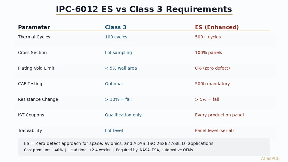
IPC-6012 ES (Enhancement Supplement) adds mandatory requirements beyond Class 3 for PCBs used in space, military avionics, and safety-critical automotive applications. Key additions include 500-cycle thermal shock testing (versus 100 cycles for Class 3), 4-point microresistance measurements on every via type, 100% cross-section inspection of HDI microvias, CAF resistance testing, and traceability to individual panel-level process parameters. These requirements reflect the zero-defect expectation of applications where field failure is not acceptable.
Understanding IPC-6012 Performance Classes
IPC-6012, the qualification and performance specification for rigid printed boards, defines a tiered system of requirements based on end-use reliability expectations. Most engineers are familiar with the three standard classes:
- Class 1 — General Electronic Products (consumer electronics, non-critical applications)
- Class 2 — Dedicated Service Electronic Products (communications equipment, industrial controls)
- Class 3 — High-Reliability Electronic Products (military, medical, critical infrastructure)
What many design teams overlook is the existence of additional performance tiers that extend beyond Class 3. The IPC-6012 ES (Enhancement Supplement) — sometimes referenced as “Class 3/A” or “Space Addendum” depending on the revision — codifies requirements for applications where even Class 3’s statistical-sampling approach to quality is insufficient.
Where Class 3 Falls Short
Class 3 was designed for military and medical products where reliability is important but statistical process control provides adequate confidence. Its underlying philosophy accepts:
- Lot-based sampling — cross-section a few coupons per lot, extrapolate to the population
- Pass/fail thresholds — minor plating voids (< 5% of wall) are acceptable
- 100-cycle thermal stress — validates survival through expected thermal excursions
- Group A/B/C testing — progressive qualification at decreasing sample sizes
For most mil/aero products, this works. The MTBF requirements can be met with process control and periodic verification.
But for applications where a single interconnect failure causes loss of mission (satellite), loss of life (fly-by-wire avionics), or multi-million-dollar recalls (autonomous vehicle ECUs), the statistical residual risk in Class 3 is unacceptable.
IPC-6012 ES: The Zero-Defect Supplement
The ES addendum transforms PCB qualification from statistical acceptance to deterministic verification. Its key additions:
1. Thermal Endurance: 500 Cycles Minimum
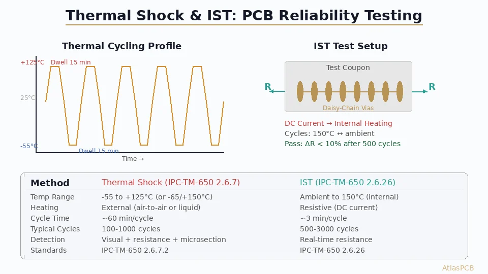
Where Class 3 requires 100 thermal cycles (-55°C to +125°C with 10-minute dwells), ES mandates 500 cycles — representing 5× the lifetime stress. Some programs specify 1000 cycles for 20-year space missions or nuclear applications.
The test methodology also differs:
- Heating rate: ≥ 10°C/minute (vs ≥ 5°C/min for Class 3)
- Monitoring: Continuous resistance measurement during cycling (not just pre/post)
- Failure criterion: > 5% resistance increase from baseline (vs > 10% for Class 3)
This rigorous thermal cycling reveals latent defects that survive 100 cycles but fail at 200–400: corner cracks in barrel plating, delamination initiation at glass-bundle boundaries, and stress-migration-induced opens.
2. Via Integrity: 100% Verification
Class 3 permits lot sampling for microsection evaluation — typically 1 coupon per panel or 1 per lot depending on panel count. ES requires:
- Every via type on a product panel must be represented in test coupons
- 100% of panels must be cross-sectioned (not just representative samples)
- Microresistance (4-point probe) on dedicated IST coupons per panel
- Zero tolerance for barrel-crack indications in any cross-section
For HDI microvias (laser-drilled, typically < 150 μm), ES adds:
- 100% X-ray inspection of via fill quality
- Mandatory stacked-via chain testing (for designs using stacked microvias)
- Separate qualification for each via-in-pad type
3. CAF Resistance Testing
Conductive Anodic Filament (CAF) growth is a catastrophic failure mode where copper ions migrate along glass-resin interfaces under bias and humidity, eventually creating shorts between adjacent vias or traces.
ES mandates CAF testing per IPC-TM-650 Method 2.6.25:
- Conditions: 85°C / 85% RH, 100V bias
- Duration: 500 hours minimum (some programs require 1000 hours)
- Acceptance: Resistance must remain > 10⁸ Ω throughout
- Via spacing tested: Minimum design-rule spacing as used on the product
This catches process issues invisible to other testing — drill smear residue, incomplete desmear, glass-bundle damage — that create future CAF paths.
4. Surface Insulation Resistance (SIR)
While Class 3 includes SIR testing, ES extends the requirements:
- Extended duration: 500 hours (vs 96 hours standard)
- Tighter acceptance: > 10⁹ Ω (vs > 10⁸ Ω)
- Product-specific patterns: Must test at actual minimum spacing used in design
- Both cleaned and as-received samples if no-clean flux will be used in assembly
5. IST (Interconnect Stress Testing) Coupons
IST applies rapid thermal cycling using resistive heating of the copper interconnect itself, inducing stress specifically in via barrels and capture pads. ES requires:
- IST coupons on every production panel (not just qualification lots)
- Pass criteria: Survive 500+ IST cycles to 150°C
- Via chain configurations: Must include worst-case layer pairs
- Traceability: Each panel’s IST result linked to production data
6. Documentation and Traceability
ES adds extensive traceability requirements:
- Individual panel serialization
- Process parameter records per panel (drill speeds, plating current density, lamination profile)
- Material lot traceability (laminate, prepreg, foil)
- Operator qualification records
- Complete inspection data package delivered with product
ATLAS PCB — MILITARY & AEROSPACE QUALIFIED
IPC-6012 Class 3 & ES Manufacturing
Our certified facilities support full IPC-6012 ES qualification including 500-cycle thermal testing, 100% IST, and complete panel-level traceability. AS9100D and IATF 16949 certified.
Request Aerospace PCB Quote →Automotive ADAS: The New ES Frontier
Historically, ES requirements were confined to space and military. The rise of autonomous driving has changed that. ADAS ECUs (radar processors, lidar controllers, sensor fusion computers) increasingly invoke ES-equivalent testing because:
- ISO 26262 ASIL D — Safety Integrity Level D requires demonstration of systematic fault elimination, which maps directly to ES’s zero-defect approach
- 15-year/300,000 km lifetime — comparable thermal cycle count to aerospace
- Vibration environments — automotive vibration profiles (random + sinusoidal) stress via interconnects similarly to thermal cycling
- Underhood temperatures — coolant module PCBs see -40°C to +150°C, matching mil-spec thermal ranges
- Volume implications — unlike aerospace (tens to hundreds of boards), automotive runs thousands per month, requiring production-compatible ES processes
Automotive Adaptations of ES
Several automotive OEMs (Bosch, Continental, ZF) have developed their own “ES-equivalent” specifications that adapt the aerospace philosophy to automotive production rates:
- Coupon-per-panel remains mandatory, but automated cross-section analysis (AI-powered image recognition) enables 100% inspection at production speeds
- IST testing is performed on-line with results feeding directly to MES (Manufacturing Execution Systems)
- CAF testing is shortened to 250 hours but with tighter spacing (closer to production minimums)
- Thermal cycling uses automotive profiles (-40°C to +150°C, faster ramp rates than mil-spec)
Manufacturing Impact
Achieving ES compliance requires process capabilities beyond standard high-reliability manufacturing:
Drilling
- Positional accuracy: ±25 μm (vs ±50 μm for Class 3)
- Hole wall roughness: < 25 μm Ra (requiring optimized feed/speed parameters)
- Drill wear monitoring: Mandatory hit-count tracking with reduced limits
Plating
- Via fill: 100% planarized fill (IPC-4761 Type VII) for all blind vias
- Barrel thickness: ≥ 25 μm average with ≥ 20 μm minimum (no exceptions)
- Uniformity: Throwing power ratio > 0.8 for aspect ratios > 8:1
- Void tolerance: 0% — any internal void is cause for rejection
Lamination
- Resin flow control: ±5% of target (prevents resin-starved areas that enable CAF)
- Temperature uniformity: ≤ 3°C variation across panel during cure
- Vacuum quality: < 5 mbar during press cycle (eliminates entrapped air)
Inspection
- Cross-section frequency: 100% of panels (automated)
- X-ray inspection: 100% of filled/plugged vias
- AOI resolution: < 10 μm for trace width verification
- Electrical test: 100% net test (flying probe or fixture) plus dedicated via-chain continuity
Cost-Benefit Analysis
For a typical 8-layer HDI board:
| Parameter | Class 3 | ES Class |
|---|---|---|
| Base fabrication cost | $80–120/board | $110–170/board (+40%) |
| Test coupon area | 5% of panel | 12% of panel |
| Lead time | 3–4 weeks | 5–7 weeks |
| Documentation package | Standard CoC | Full data package (50+ pages) |
| Panel yield | 85–92% | 75–85% (tighter accept) |
The 40% cost premium is significant for high-volume automotive, which is why OEMs work with fabricators to develop production-efficient ES processes rather than simply applying aerospace methods unchanged.
Implementation Roadmap
For design teams transitioning to ES requirements:
- Early engagement — involve your PCB fabricator during schematic/layout phase, not after Gerber release
- Design for testability — include IST chains, CAF coupons, and cross-section targets in the PCB design (not afterthought additions)
- Material pre-qualification — select laminates with demonstrated CAF resistance at your operating voltage and spacing
- Via design rules — apply ES-specific rules (minimum annular ring 75 μm, via-to-via spacing ≥ conductor pitch × 1.5)
- Documentation — specify ES requirements in your fabrication drawing using IPC-D-325 symbology
Further Reading
- [IPC-A-610 Class 3 Inspection: Workmanship Standards for High-Reliability PCBs]/blog/ipc-a-610-class-3-inspection-workmanship-high-reliability/)
- [IPC-A-600 Class 2 vs Class 3 PCB Acceptability Standards]/blog/ipc-a-600-class-2-vs-class-3-pcb-acceptability/)
- [PCB Test Coupon Design and IPC Standards]/blog/pcb-test-coupon-design-ipc-standards/)
- [PCB Via Reliability Testing: Thermal Cycling and IST Methods]/blog/pcb-via-reliability-testing/)
Designing for IPC-6012 ES compliance? AtlasPCB provides DFM reviews specifically for high-reliability class requirements and can identify potential ES non-conformances before fabrication. Contact our engineering team →
About AtlasPCB — We specialize in complex PCB manufacturing for HDI, RF, and high-reliability applications. Explore our aluminum and metal-core PCB services, or get an full PCB manufacturing capabilities . Every order includes free engineering review. Get your quote.
Reviewed by AtlasPCB Engineering Team — IPC-certified manufacturing specialists with 15+ years of production experience in HDI, RF, and high-reliability PCB fabrication. Content based on factory floor data and real customer design reviews.
Frequently Asked Questions
What is the difference between IPC-6012 Class 3 and IPC-6012 ES?
Which industries require IPC-6012 ES compliance?
How does IPC-6012 ES affect PCB manufacturing cost and lead time?
- ipc-6012
- ipc standards
- automotive pcb
- aerospace pcb
- reliability testing
- qualification
- class 3
- thermal cycling
- microsection