· AtlasPCB Engineering · Engineering · 9 min read
Multilayer PCB Cost Breakdown: What Drives Pricing from 4 to 30 Layers
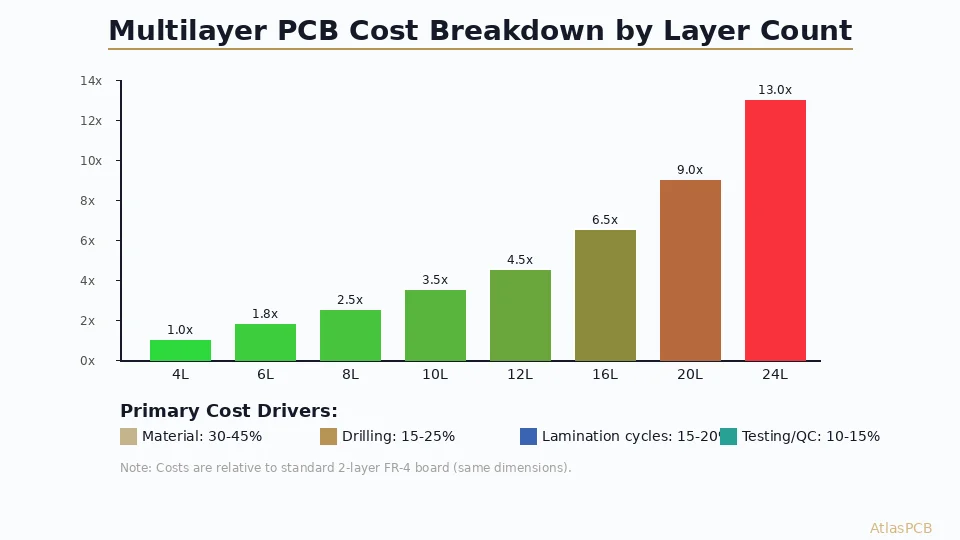
Understanding multilayer PCB cost requires knowing what fabrication steps multiply with layer count. This pricing guide breaks down the cost drivers — lamination cycles, material, drilling, and testing — with real price ranges for 4-layer through 30-layer boards in production quantities.
Quick Answer
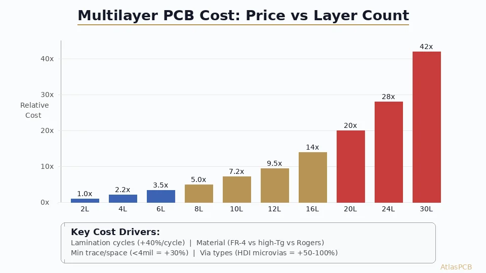
Multilayer PCB cost scales non-linearly with layer count. A 4-layer board costs approximately 2.2x a 2-layer equivalent, while 8-layer costs 5x, 16-layer costs 14x, and 30-layer costs 40-45x. The primary cost drivers are lamination cycles (each adds 40% to base processing cost), material consumption (prepreg and core sheets), drilling time (more layers = more via types), and electrical testing complexity. HDI construction with microvias adds 50-100% on top of the layer-count-based pricing.
Quick Reference: Multilayer PCB Pricing Table
| Layer Count | Relative Cost | Lamination Cycles | Typical $/pcs (100x100mm, qty 50) | Lead Time |
|---|---|---|---|---|
| 2-layer | 1x | 0 | $1.50-3.00 | 3-5 days |
| 4-layer | 2.2x | 1 | $3.50-6.00 | 5-7 days |
| 6-layer | 3.5x | 2 | $6.00-10.00 | 7-10 days |
| 8-layer | 5x | 2-3 | $8.00-15.00 | 8-12 days |
| 10-layer | 7.2x | 3-4 | $12.00-22.00 | 10-14 days |
| 12-layer | 9.5x | 4-5 | $16.00-28.00 | 12-16 days |
| 16-layer | 14x | 5-6 | $25.00-45.00 | 14-18 days |
| 20-layer | 20x | 6-8 | $40.00-70.00 | 16-21 days |
| 24-layer | 28x | 8-10 | $55.00-95.00 | 18-24 days |
| 30-layer | 42x | 10-12 | $85.00-150.00 | 21-28 days |
Pricing assumes: standard FR-4, 1oz copper, 4/4mil trace/space, mechanical drills only, no impedance control. Add 20-40% for impedance-controlled designs, 50-100% for HDI microvias, 100-300% for Rogers/specialty materials.
Understanding the Non-Linear Cost Curve
PCB pricing does not scale linearly with layer count because the manufacturing process compounds in complexity. Going from 2 layers to 4 layers adds one lamination cycle and roughly doubles the material — a 2.2x cost increase. But going from 16 to 20 layers adds two more lamination cycles on top of an already complex process, with tighter registration requirements and higher defect risk on every subsequent pressing step.
The compounding effect happens because each lamination cycle is not just “pressing another sheet of copper.” It requires: oxide treatment or brown/black oxide surface preparation on previously etched inner layers, precise layer-to-layer registration using optical targets (with tighter tolerance each cycle because errors accumulate), a full press cycle at 375F for 2-3 hours, post-lamination inspection for delamination and registration, and sometimes re-drilling of registration holes for subsequent imaging steps.
In our production facility, we track yield loss by layer count. A standard 4-layer board achieves 96-98% first-pass yield. At 12 layers, yield drops to 90-93%. At 20+ layers, yield ranges from 80-88% depending on design complexity. These yield losses are built into the unit price — when 12% of panels are scrapped at the 20-layer stage, the cost of those lost panels is distributed across the good units.
MULTILAYER PCB MANUFACTURER
Get Exact Pricing for Your Layer Count
Upload your Gerber files or stackup specification for an instant quote. We fabricate 1 to 30 layers with impedance control, HDI microvias, and controlled dielectric thickness.
Get Instant Quote ›
Cost Driver 1: Lamination Cycles (40% of cost per cycle added)
Each lamination press cycle is the most expensive individual step in multilayer fabrication. The press equipment costs $2-5 million, operates at 375F under 200-400 psi for 2-3 hours per cycle, and consumes significant energy. A 4-layer board requires one press cycle. A 12-layer board requires 4-5 cycles, each adding cost not just for the press time but for the associated preparation steps.
The sequence for an 8-layer board illustrates why cycles compound cost. First, the inner core layers (L3/L4 and L5/L6) are imaged and etched separately. Then they are laminated together with L4/L5 prepreg in the first press cycle. After drilling registration holes and surface preparation, outer layers (L1/L2 and L7/L8 prepreg) are added in a second press cycle. Each cycle adds material handling, registration verification, and the risk of defects that scraps all prior work invested in that panel.
For HDI boards, the penalty is even steeper. A 2+N+2 HDI structure requires the N-layer core to be built first (requiring its own lamination cycles), then two additional sequential lamination cycles to add the HDI buildup layers — one per side. Each HDI lamination cycle adds approximately 50-60% to unit cost because it also includes laser drilling and microvia plating between cycles.
Cost Driver 2: Material Consumption
Material cost scales with layer count but is not the dominant cost driver unless specialty materials are involved. Standard FR-4 copper-clad laminate costs $15-25 per panel (18x24 inches, 1oz copper). Prepreg sheets cost $8-15 per ply. A 4-layer board uses 1 core + 2 prepreg plies = approximately $40 in material. A 16-layer board uses 7 cores + 8 prepreg plies = approximately $180 in material.
Where material cost becomes the primary driver is when Rogers, PTFE, or other specialty laminates are specified. Rogers 4350B costs $180-250 per panel — 8-12x the cost of FR-4. If only 2 layers of a 12-layer stackup use Rogers (common in hybrid RF designs), material cost increases by $320-500 per panel, which adds approximately $15-25 per board on a 20-up panel.
Controlled-dielectric prepreg (precise thickness for impedance targeting) costs 20-40% more than standard prepreg but is required for any impedance-controlled design. Since most multilayer boards above 6 layers include at least some impedance control, this premium is nearly universal.
Cost Driver 3: Drilling Complexity
Drilling represents 15-25% of total multilayer PCB fabrication cost. The cost scales with: total number of holes (more layers = more interconnect vias needed), number of different drill sizes (each size requires a tool change), and whether blind/buried vias are required.
A typical 4-layer board might have 2,000-5,000 through-holes of 3-4 different sizes. A 16-layer board with the same circuit complexity might have 10,000-20,000 holes due to additional stitching vias, ground vias, and signal vias that were previously unnecessary on fewer layers. At our drilling throughput of 300-400 hits per minute, that is the difference between 10 minutes and 50+ minutes of drilling per panel.
Blind and buried vias dramatically increase drilling cost because they require multiple drill programs at different stages of the fabrication process. Buried vias (connecting inner layers only) must be drilled on the inner core before lamination. Blind vias (connecting outer to inner) are drilled after lamination using controlled-depth drilling or laser. Each via type adds a drilling setup, registration verification, and dedicated plating step.
From a cost optimization perspective, the single most effective technique is to design with through-hole vias wherever possible and use back-drilling to remove via stubs on high-speed signals. Back-drilling adds modest cost ($0.50-1.00/board in most cases) but avoids the 50-80% cost premium of true blind/buried via construction.
HDI PCB MANUFACTURER
Need HDI Without HDI Pricing?
Our engineers can often suggest through-hole + back-drill solutions that achieve similar signal integrity to blind vias at 40-60% lower cost. Ask about design optimization during quoting.
Compare Pricing Options ›Cost Driver 4: Electrical Testing
Electrical testing (continuity and isolation verification) scales quadratically with net count and layer count. A 4-layer board with 500 nets requires testing approximately 2,000 test points. A 16-layer board with the same net count might have 6,000+ test points due to additional via connections and internal layer nodes.
For prototype quantities (1-25 panels), flying probe testing is standard. The test time scales linearly with test point count — 5,000 points takes approximately 3-5 minutes per board. At $0.50-1.50 per minute of test time, a complex 16-layer board might cost $3-5 per board in testing alone.
For production quantities (100+ panels), a custom test fixture (bed-of-nails) reduces per-board test time to seconds but requires $2,000-5,000 fixture investment. The breakeven point is typically 200-500 boards, after which fixture testing is dramatically cheaper per unit.
Practical Cost Optimization Strategies
Based on our quoting data, here are the modifications that most significantly reduce multilayer PCB cost, ranked by impact:
1. Increase minimum trace/space (Impact: -15-25%) Moving from 3/3mil to 4/4mil relaxes imaging tolerance, reduces etch defects, and improves yield. If your routing allows it, this single change can reduce price by 15-25% because it moves the board from “advanced” to “standard” process capability at most factories.
2. Eliminate unnecessary via types (Impact: -20-50%) Convert blind vias to through-holes + back-drilling where signal integrity allows. Eliminate buried vias if layer reassignment can route those connections as through-holes. Each via type eliminated removes a drill/plate cycle from the process.
3. Optimize board dimensions for panelization (Impact: -10-20%) A 90x90mm board arrays 4x5 = 20 pieces on a standard 18x24” panel. A 95x95mm board arrays only 4x4 = 16 pieces — same panel cost, 20% fewer boards. Small dimension changes can significantly improve material utilization.
4. Relax impedance tolerance (Impact: -5-15%) Standard impedance tolerance is +/-10%. Requesting +/-5% tightens manufacturing requirements and increases fallout. If your simulation shows 10% tolerance is acceptable, do not over-specify.
5. Consider alternative constructions (Impact: variable) Sometimes a 10-layer board with through-hole vias is cheaper than an 8-layer HDI (2+4+2) board — even though it has more layers — because it avoids sequential lamination. Our engineers can quote both approaches and help you decide which architecture minimizes cost for your performance requirements.
Volume Pricing Breakdown
| Quantity | Typical Discount vs Prototype | Why |
|---|---|---|
| 1-5 pcs | Baseline (prototype pricing) | Setup cost amortized over few units |
| 10-25 pcs | -20-30% | Panel fills up, setup is amortized |
| 50-100 pcs | -40-50% | Multiple panels, drilling programs cached |
| 500-1000 pcs | -55-65% | Dedicated tooling, material volume buy |
| 5000+ pcs | -65-75% | Blanket material order, optimized process flow |
The most dramatic price improvement happens between 5 pieces and 100 pieces. If you are ordering 5 prototypes at $45 each, the same board in quantities of 100 might cost $15-20 each — a 55-65% reduction. This is because the fixed costs (CAM processing, tooling, setup, test fixture) are amortized over more units.
PCB MANUFACTURER FOR AEROSPACE
Transparent Pricing, No Hidden Fees
Our quoting system provides detailed cost breakdown by layer count, material, and process options. Compare different constructions side-by-side to find the optimal balance of performance and cost.
Get Detailed Quote ›ATLASPCB
Know Exactly What Your Board Will Cost
Upload your Gerber files for instant pricing. Our system provides line-item cost breakdown showing exactly where your money goes — material, lamination, drilling, testing, and finishing. No surprises.
Get Instant Quote ›
Reviewed by AtlasPCB Engineering Team — 15+ years in advanced PCB fabrication for RF, HDI, and rigid-flex applications.
Related Reading:
About AtlasPCB — We specialize in complex PCB manufacturing for HDI, RF, and high-reliability applications. Explore our HDI PCB manufacturing capabilities, multilayer PCB fabrication up to 30 layers, or get an instant online PCB quote . Every order includes free engineering review. Get your quote.
Reviewed by AtlasPCB Engineering Team — IPC-certified manufacturing specialists with 15+ years of production experience in HDI, RF, and high-reliability PCB fabrication. Content based on factory floor data and real customer design reviews.
Frequently Asked Questions
How much does an 8-layer PCB cost compared to 4-layer?
What is the biggest cost driver in multilayer PCBs?
Does HDI add cost beyond the layer count?
How can I reduce multilayer PCB cost without reducing layers?
At what volume does multilayer PCB pricing improve significantly?
- multilayer PCB cost
- PCB pricing
- HDI PCB cost
- PCB manufacturer
- layer count