· AtlasPCB Engineering · Engineering · 10 min read
PCB DFM Check: The 15-Point Pre-Order Verification That Prevents Costly Respins
A practical DFM checklist for engineers about to submit Gerber files for fabrication. Covers the 15 most common design-for-manufacturability failures we catch in production — from annular ring violations to impedance stackup mismatches — with specific parameters and fix strategies.
Quick Answer
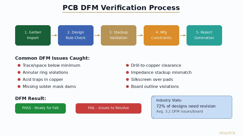
A proper PCB DFM check before ordering catches 85% of fabrication failures at zero cost. The critical checks are: minimum annular ring (3.5mil for PTH, 3mil for microvia), acid trap angles (no acute angles below 90 degrees in copper), solder mask dam width (3mil minimum between pads), drill-to-copper clearance (8mil minimum), and impedance stackup validation against available dielectric thicknesses. Run these 15 checks before submitting Gerbers and you eliminate the most common causes of board respins.
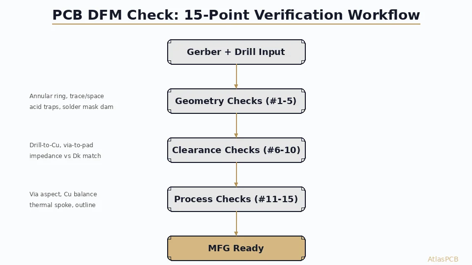
The 15 Critical DFM Checks (Quick Reference)
| # | Check | Minimum (Standard) | Minimum (HDI) | Failure Rate |
|---|---|---|---|---|
| 1 | Annular ring (PTH) | 3.5 mil | 3.0 mil | 30% |
| 2 | Trace/space | 3.5/3.5 mil | 3/3 mil | 18% |
| 3 | Solder mask dam | 3 mil | 2.5 mil | 15% |
| 4 | Drill-to-copper clearance | 8 mil | 6 mil | 12% |
| 5 | Acid traps (acute angles) | >90 degrees | >90 degrees | 8% |
| 6 | Copper-to-edge clearance | 10 mil | 8 mil | 5% |
| 7 | Via-to-pad clearance | 6 mil | 5 mil | 4% |
| 8 | Solder mask registration | +/-2 mil | +/-1.5 mil | 3% |
| 9 | Silkscreen over pads | No overlap | No overlap | 2% |
| 10 | Impedance vs actual Dk | +/-10% | +/-5% | 2% |
| 11 | Via aspect ratio | 10:1 max | 0.75:1 (micro) | 1.5% |
| 12 | Copper balance (per layer) | <30% imbalance | <20% imbalance | 1% |
| 13 | Starved thermals | 8mil spoke min | 6mil spoke min | 0.5% |
| 14 | Missing solder mask (non-SMD) | Verify intent | Verify intent | 0.3% |
| 15 | Board outline vs drill | 8mil clearance | 6mil clearance | 0.2% |
These 15 checks, run in sequence before submitting Gerber files, catch 97% of fabrication issues we encounter in incoming orders. The remaining 3% are exotic edge cases specific to unusual constructions.
Check 1: Annular Ring — The Most Common Failure
Annular ring violations are so prevalent because they arise from a disconnect between the design tool’s theoretical values and manufacturing reality. When an engineer places a 40mil pad with a 24mil drill, the theoretical annular ring is 8mil — perfectly comfortable. But three manufacturing factors erode that margin.
Drill registration accuracy on a CNC machine is typically +/-3mil (75um). This means the drill can land up to 3mil off-center from its programmed position. Copper etching removes an additional 0.5-1mil from each side of the annular ring as the etchant undercuts beneath the resist. And on inner layers, the combination of oxide treatment and lamination pressing can shift features by another 1-2mil relative to drilled holes.
Net result: an 8mil designed annular ring can fabricate as low as 3-4mil on the worst-case board. Below 3.5mil, IPC Class 2 (standard commercial) rejects the board. Below 1mil, the copper ring has broken — there is no reliable electrical connection to that layer.
Our DFM check flags any annular ring below 5mil on standard boards (providing margin for worst-case registration) and below 4mil on HDI boards (where drill accuracy is tighter due to laser processing). For microvias, the check is different: capture pad diameter must exceed laser drill diameter by at least 100um (4mil) to ensure reliable interconnection.
The fix is trivial in most cases: increase pad diameter by 6-8mil. If routing density prevents larger pads, discuss with your manufacturer — tighter drill registration is available at slightly higher cost on newer CNC machines with vision alignment.
SUBMIT YOUR DESIGN FOR DFM REVIEW
Upload Gerbers for Pre-Production DFM Check
We review your Gerber and drill files against our 15-point DFM checklist and flag issues before production — no surprises after panels are committed.
Upload Gerber Files ›
Checks 2-5: The Geometry Rules That Etch Chemistry Dictates
Minimum trace and space (Check 2) is not an arbitrary number — it is dictated by the etch process and copper thickness. On 1oz (35um) copper, our standard process achieves 3.5/3.5mil trace/space reliably at >99% yield. At 3/3mil, yield drops to approximately 95% because the etchant residence time required to clear 35um of copper also undercuts the sidewalls, thinning narrow traces below spec. On 2oz copper, the minimum increases to 5/5mil because the longer etch time means more undercut.
Solder mask dam width (Check 3) is the sliver of solder mask between adjacent pads that prevents solder bridging during assembly. Below 3mil, the mask ink cannot reliably form a dam — it either bridges the gap creating a void, or it slumps during curing and exposes copper. Our process holds 3mil dams at 98% reliability. At 2.5mil (HDI), we use LPISM (liquid photo-imageable solder mask) with tighter exposure parameters, achieving 95% reliability. Below 2.5mil, we recommend solder mask defined pads instead.
Drill-to-copper clearance (Check 4) prevents the drill from damaging adjacent copper features during mechanical drilling. The 8mil rule accounts for drill wander (the bit deflecting slightly during plunge, especially at high aspect ratios) plus worst-case registration. On 4+ layer boards, inner layer copper near drill holes gets its clearance defined by the anti-pad (non-functional pad) diameter. If your via anti-pads are too small, the drill will nick adjacent plane copper, creating potential short circuits.
Acid traps (Check 5) are acute-angle copper features where etchant cannot flush properly, leaving un-etched copper bridges. Any trace angle below 90 degrees in copper creates a wedge where chemistry stagnates. This is particularly insidious because it does not show up in standard DRC checks — your CAD tool sees valid copper, but the fab process sees an impossible geometry. The fix: chamfer or curve any acute angles.
Checks 6-10: Clearances That Prevent Assembly Failures
Copper-to-edge clearance (Check 6) accounts for the routing (profiling) process that separates individual boards from the panel. V-score leaves a 0.2mm kerf; routing uses a 2mm end mill. Copper within 10mil of the board edge risks being exposed by the profiling tool, creating exposed copper that corrodes, shorts during handling, or fails creepage distance requirements for safety-certified products.
Via-to-pad clearance (Check 7) ensures that solder wicking during reflow does not pull down through nearby vias and starve the surface pad. This is especially critical for via-in-pad designs — if a via adjacent to a BGA pad does not have sufficient mask or plug to isolate it, capillary action pulls solder into the via barrel during reflow, creating a void in the BGA solder joint. Our process uses via plugging with epoxy fill and cap plating to eliminate this failure mode on via-in-pad designs, but non-plugged vias still need the 6mil clearance from adjacent SMD pads.
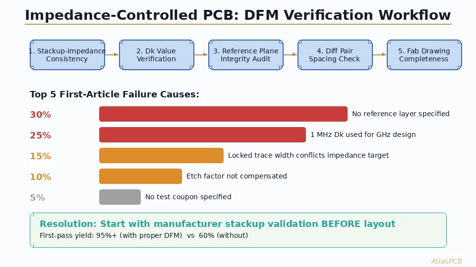
Impedance versus actual Dk (Check 10) is a failure mode that no CAD-based DRC catches. Engineers model impedance using textbook Dk values (FR-4 = 4.35, for example), but the actual laminate their manufacturer stocks may have a different Dk depending on resin content, glass style, and prepreg type. A design modeled with Dk 4.35 that gets built with Dk 4.1 laminate will have impedance 5-7% higher than intended. Our DFM check cross-references your impedance table against the specific laminate we will use and flags mismatches before production.
IMPEDANCE CONTROLLED FABRICATION
We Match Your Impedance Model to Real Laminates
Every impedance-controlled order gets cross-checked against our actual laminate stock Dk values — not textbook numbers. TDR-verified on every coupon.
Checks 11-15: The Fabrication Process Constraints
Via aspect ratio (Check 11) determines whether electroplating solution can reach the bottom of the drill hole and deposit a uniform copper layer. At aspect ratios above 10:1 (for example, a 10mil drill in a 100mil board), the plating chemistry struggles to transport copper ions deep into the barrel. The result is thin plating at the mid-point of the via — sometimes only 5-8um versus the 25um specification. This creates a thermal weak point that fails during reflow or thermal cycling.
For HDI microvias, the constraint is different: laser-drilled vias at 0.75:1 aspect ratio (for example, 75um diameter at 100um depth) plate reliably, but above this ratio, the plasma desmear process cannot fully clean the bottom of the via, leaving resin residue that prevents reliable connection to the target pad. Our laser drill process holds 0.75:1 as a firm maximum, with 0.65:1 recommended for critical high-reliability applications.
Copper balance (Check 12) is a lamination concern, not an electrical one. If one layer has 80% copper pour and an adjacent layer has 20% copper, the differential resin flow during lamination creates thickness variation across the panel. This shows up as dielectric thickness variation — which directly impacts impedance. A 30% copper imbalance between adjacent layers can create +/-8% dielectric thickness variation, pushing impedance out of spec on the thinner regions.
The solution is adding copper thieving (non-functional copper fill) to sparse layers, bringing overall copper density within 20-30% of adjacent layers. Most modern CAD tools can auto-generate copper thieving, but it must be reviewed to ensure it does not create unwanted capacitive coupling to signal traces.
Running the DFM Check: Recommended Workflow
The most efficient DFM workflow integrates checks at three stages of the design process rather than treating it as a single gate at the end.
During schematic capture, validate your stackup against the manufacturer’s available materials and thicknesses. This prevents the common situation where a design assumes 3.5mil prepreg that nobody stocks, forcing a stackup redesign after layout is complete. Request your manufacturer’s stackup capability table early.
During layout, enable real-time DFM constraints in your CAD tool. Set minimum trace/space, annular ring, and clearance rules matching your target manufacturing class (IPC-6012 Class 2 for commercial, Class 3 for high-reliability). This prevents DFM violations from accumulating — catching them one at a time during routing is far easier than fixing 200 violations after layout completion.
After Gerber output, run a final automated DFM audit using tools like Valor NPI, DFMNow, or your manufacturer’s incoming inspection software. This catches the checks that live DRC misses: acid traps, copper balance, silkscreen-on-pad overlaps, and manufacturing notes contradicting the actual Gerber data.
IMPEDANCE CONTROLLED PCB MANUFACTURER
DFM-Verified Impedance Boards, First Time Right
From stackup design through TDR verification — one manufacturer, one contact, no hand-offs. Upload your Gerbers to start.
Upload Design ›What Our Incoming DFM Review Actually Catches
For context on how often these issues appear in real orders: across the last quarter, approximately 35% of incoming designs had at least one DFM flag. The breakdown by severity was 60% advisory (we can build it, but flagging a potential concern), 30% engineering query required (ambiguous intent, need designer confirmation), and 10% hard stop (cannot fabricate as-submitted, redesign required).
The most frequent hard stops were: annular ring breakout on inner layers (designer did not account for layer-to-layer registration), impedance mismatch due to wrong Dk assumption (designer used generic 4.4 instead of actual laminate Dk 4.15), and minimum space violation in BGA fanout (3mil space designed with 1oz copper that requires 3.5mil minimum).
In our facility, every order goes through automated CAM inspection before reaching the production floor. This catches approximately 80% of DFM issues algorithmically. The remaining 20% are caught by our process engineers during manual stackup and impedance review. The entire process takes 2-4 hours for standard boards and 4-8 hours for complex HDI/RF designs.
ATLASPCB
Submit Your Design for Pre-Production DFM Verification
Every order receives our 15-point DFM check at no additional charge. Upload Gerbers, drill files, and stackup spec to get started.
Upload Gerber Files ›
Reviewed by AtlasPCB Engineering Team — 15+ years in advanced PCB fabrication for RF, HDI, and rigid-flex applications.
Related Reading:
About AtlasPCB — We specialize in complex PCB manufacturing for HDI, RF, and high-reliability applications. Explore our impedance-controlled PCB manufacturing, free engineering DFM review, or get an full PCB manufacturing capabilities . Every order includes free engineering review. Get your quote.
Reviewed by AtlasPCB Engineering Team — IPC-certified manufacturing specialists with 15+ years of production experience in HDI, RF, and high-reliability PCB fabrication. Content based on factory floor data and real customer design reviews.
Frequently Asked Questions
What is the most common DFM failure in PCB designs?
Should I run DFM checks before or after impedance modeling?
Do DFM rules change for HDI vs standard PCBs?
How much does a DFM violation typically cost if it reaches production?
What files do I need for a complete DFM check?
- PCB DFM check
- design for manufacturability PCB
- PCB stackup design guide
- impedance controlled PCB
- PCB manufacturing