· Priya Nair · Engineering · 6 min read
BGA X-Ray Void Analysis: Xray Ipc
Master BGA solder joint void analysis using X-ray inspection. Understand IPC-7095 acceptance criteria, void percentage calculations, and how to distinguish process voids from reliability-threatening defects.
Quick Answer
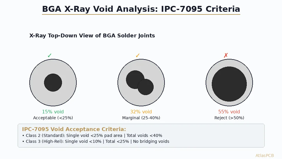
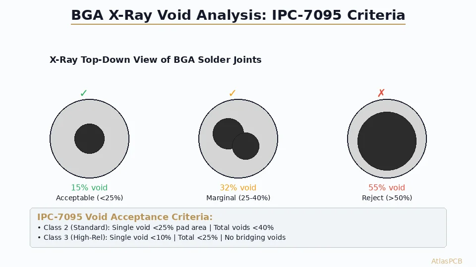
IPC-7095 defines BGA solder void acceptance as: Class 2 allows individual voids up to 25% of pad area with total voiding below 40%, while Class 3 (high-reliability) limits individual voids to 10% and total voiding to 25%. Voids are measured from 2D X-ray images by calculating void area relative to the solder ball pad area.
Why BGA Void Analysis Matters
Ball Grid Array (BGA) packages dominate modern PCB assembly — from mobile processors to automotive ECUs and networking ASICs. Unlike leaded components where solder joints are visually inspectable, BGA connections are hidden beneath the package body. X-ray inspection is the only non-destructive method to evaluate BGA solder joint quality.
Voids — gas pockets trapped within solder joints — are the most common BGA anomaly detected during X-ray inspection. Understanding when voids represent a genuine reliability risk versus an acceptable process artifact is critical for yield optimization and quality decisions.
Understanding IPC-7095: The BGA Standard
IPC-7095 “Design and Assembly Process Implementation for BGAs” provides the industry-standard framework for BGA void acceptance. The key sections addressing voids are:
Void Classification by Size
IPC-7095 defines void percentage as:
Void% = (Sum of void areas / Pad area) × 100
Where pad area is the designed copper pad area (not the solder ball diameter).
Class 2 (Standard Electronic Products)
- Individual void: ≤25% of pad area
- Total voiding: ≤40% of pad area (sum of all voids)
- No single void touching both pad interfaces (top and bottom)
- Applications: Consumer electronics, commercial computing, telecom
Class 3 (High-Reliability Products)
- Individual void: ≤10% of pad area
- Total voiding: ≤25% of pad area
- No voids at pad-to-solder interface (interface voids are more critical)
- No voiding that creates a continuous path across the joint
- Applications: Aerospace, medical devices, military, automotive safety
Process Indicator Levels
Beyond pass/fail, IPC-7095 establishes process control levels:
| Level | Total Void % | Action Required |
|---|---|---|
| Target | <10% | Normal production |
| Acceptable | <25% (Class 3) / <40% (Class 2) | Monitor trend |
| Process Alert | 25-40% (Class 3) / 40-50% (Class 2) | Investigation needed |
| Reject | >40% (Class 3) / >50% (Class 2) | Rework or scrap |
X-Ray Inspection Methodology
2D Transmission X-Ray
The standard inspection method for production BGA void analysis:
Equipment requirements:
- Tube voltage: 90-130 kV (dependent on board thickness)
- Geometric magnification: 10-50×
- Detector resolution: ≤5 μm feature size
- Oblique angle capability: 0-70° tilt for layer separation
Measurement procedure:
- Acquire top-down (0°) image of BGA area
- Identify solder ball boundaries using grayscale thresholding
- Calculate pad area (circle fit or actual pad geometry)
- Identify voids as darker regions within ball area
- Calculate individual and total void percentages
- Compare against IPC-7095 class requirements
Oblique Angle Inspection
Tilting the X-ray beam to 30-60° separates overlapping features:
- 30° tilt: Separates top and bottom BGA rows in double-sided assemblies
- 45° tilt: Reveals head-in-pillow (HIP) defects hidden in 0° view
- 60° tilt: Exposes non-wetting conditions and collapsed/bridged balls
3D CT (Computed Tomography)
For failure analysis and critical reliability assessment:
- Creates full 3D volumetric reconstruction
- Reveals void position within joint (interface vs bulk)
- Identifies crack propagation paths post-thermal cycling
- Resolution: 1-5 μm voxel size (micro-CT)
- Throughput: 5-30 minutes per component (not suitable for 100% inspection)
Need Production BGA Assembly with X-Ray Inspection?
AtlasPCB's assembly line includes 5DX automated X-ray inspection with 100% BGA coverage. We provide void analysis reports meeting IPC-7095 Class 2/3 requirements.
Request Assembly Quote →Root Cause Analysis: Why Voids Form
Flux Outgassing (Most Common — 60-70% of Cases)
During reflow, flux activators and vehicles decompose and release gases. If the solder solidifies before these gases escape, voids remain trapped.
Contributing factors:
- Aggressive ramp rate (>2°C/sec) — insufficient time for flux activation
- Short time above liquidus (<60 sec for SAC305)
- Excessive flux volume (stencil too thick or aperture oversized)
- Low-activity flux unable to fully activate at process temperature
Mitigation:
- Optimize reflow profile: Extend soak zone (150-200°C) to 60-90 seconds
- Ensure TAL (time above liquidus) ≥ 60 seconds for SAC alloys
- Consider vacuum reflow for critical applications (reduces voids to <2%)
Moisture-Related Voiding
Moisture absorbed in PCB laminate or BGA substrate explosively vaporizes during reflow:
- FR-4 absorbs 0.1-0.3% moisture by weight
- BGA substrates (especially organic) absorb 0.05-0.15%
- At 250°C, trapped moisture generates ~20 atm pressure
Mitigation:
- Bake PCBs at 125°C for 4-8 hours before assembly
- Handle BGAs per MSL (Moisture Sensitivity Level) requirements
- Monitor factory humidity (<60% RH in assembly areas)
Via-in-Pad Voiding
When vias beneath BGA pads are not properly filled and capped:
- Solder wicks into via barrel during reflow
- Air trapped in via creates large void directly at interface
- Most critical void type — directly impacts thermal path
Mitigation:
- Specify VIPPO (Via-In-Pad Plated Over) with 100% copper fill
- Verify via fill by cross-section (target >95% fill)
- Alternative: Use dog-bone fanout to avoid via-in-pad
Pad Surface Contamination
Oxidation, organic contamination, or plating defects on pads:
- ENIG black pad (nickel hyper-corrosion) causes widespread non-wetting
- OSP shelf life exceeded (>6 months) leads to oxidation
- Solder mask residue on pad edges traps flux
Automated vs Manual Void Measurement
Automated X-Ray Inspection (AXI)
Modern AXI systems provide:
- Throughput: 100% inspection at line speed (5-15 sec/board)
- Consistency: Algorithmic void calculation eliminates operator variability
- Statistics: SPC data for trend monitoring across production lots
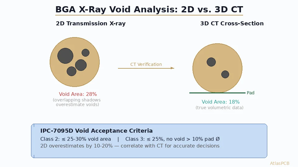
- Limitations: 2D measurement may overestimate void % when voids overlap vertically
Manual Measurement Best Practices
For failure analysis and arbitration:
- Use calibrated measurement software (not estimated percentages)
- Define ball boundary using 50% grayscale threshold
- Define void boundary using same threshold method
- Calculate area using pixel counting, not diameter estimation
- Document measurement parameters for reproducibility
Process Optimization: Reducing BGA Voids
Reflow Profile Optimization
The single most effective lever for void reduction:
| Profile Parameter | Void-Prone | Optimized |
|---|---|---|
| Ramp rate | >2.5°C/s | 1.0-1.5°C/s |
| Soak time (150-200°C) | <30 sec | 60-90 sec |
| Time above liquidus | <45 sec | 60-90 sec |
| Peak temperature | >250°C | 240-245°C (SAC305) |
| Cooling rate | >4°C/s | 2-3°C/s |
Stencil Design Impact
- Aperture reduction: 1:1 pad-to-aperture for 0.5 mm pitch; 90% for larger pitches
- Stencil thickness: 100-125 μm for fine-pitch BGA; 150 μm for 1.0+ mm pitch
- Aperture shape: Round apertures produce fewer voids than square for BGA sites
- Nano-coating: Reduces flux sticking and improves paste release
Advanced Solutions
- Vacuum reflow: Reduces voids to <2% by evacuating chamber at peak temperature
- Nitrogen atmosphere: Prevents oxidation, allowing lower peak temperatures
- Formic acid reflow: Eliminates flux entirely for ultra-low void applications
Industry Trends: Evolving Void Challenges
Package-on-Package (PoP) and 3D Stacking
Stacked packages create multiple solder layers, making void detection more complex:
- Overlapping ball images require CT or oblique angle separation
- Thermal path through multiple joints amplifies void impact
- Industry moving toward stricter <15% total void for PoP applications
Fine-Pitch BGA (≤0.4 mm)
Smaller balls have proportionally larger surface-area-to-volume ratios:
- Flux outgassing has less solder mass to escape through
- Via-in-pad becomes mandatory, increasing void risk
- Void percentage thresholds may need revision for sub-0.4mm pitch
Further Reading
- BGA Pad Design and Via-in-Pad Solder Voiding Prevention
- AOI and SPI Inspection in PCB Assembly Quality Control
- DFM Rules for Fine-Pitch BGA PCB Design
Ensure Quality BGA Assembly with AtlasPCB
Our assembly facility features automated X-ray inspection with IPC-7095 void analysis capability, vacuum reflow for critical applications, and comprehensive SPC monitoring. Whether you need Class 2 production volumes or Class 3 aerospace-grade quality, our process engineering team optimizes every parameter for your specific BGA requirements.
About AtlasPCB — We specialize in complex PCB manufacturing for HDI, RF, and high-reliability applications. Explore our HDI PCB manufacturing capabilities, PCB assembly services, or get an full PCB manufacturing capabilities . Every order includes free engineering review. Get your quote.
Reviewed by AtlasPCB Engineering Team — IPC-certified manufacturing specialists with 15+ years of production experience in HDI, RF, and high-reliability PCB fabrication. Content based on factory floor data and real customer design reviews.
Frequently Asked Questions
What causes voids in BGA solder joints?
Are all voids in BGA joints harmful to reliability?
What is the difference between 2D and CT X-ray for BGA void analysis?
- bga
- x-ray inspection
- void analysis
- ipc-7095
- solder joint
- pcb assembly
- quality control