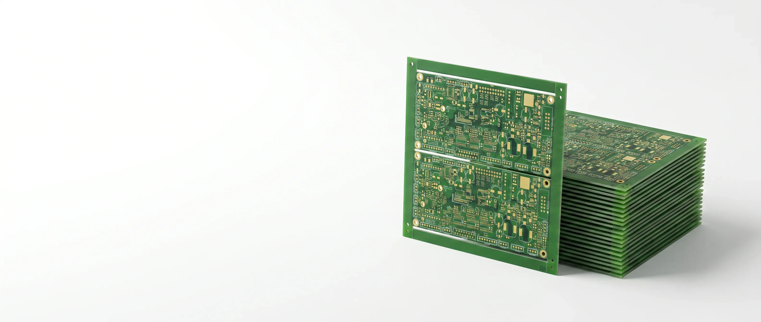
Rigid PCB Manufacturing
Multilayer PCB Manufacturer 2 to 30 Layers, Precision Built
Up to 30 layers. 3/3mil trace. ±8% impedance. Every board engineered for first-pass success.
At a Glance
What Sets Us Apart
Not Your Average Board House
We specialize in the boards that other shops struggle with.
3/3mil Fine-Pitch Routing
Break out 0.5mm BGA without HDI. Our advanced imaging and etching lines maintain consistent trace geometry at 75μm features.
±8% Impedance Control
Dielectric thickness precision with TDR verification on every controlled-impedance order. Reports ship with your boards — not on request.
Engineering Before Production
A human engineer reviews your stackup, material selection, and DFM before any panel touches a production line. Issues caught here, not at assembly.
5-Day Prototype Turnaround
Standard 5-day lead time for 1-2 layer boards. Rush options available, reducing lead time by up to 4 days (minimum 1-day turnaround).
High-TG for Lead-Free
TG170 material standard for complex multilayer builds. Survives multiple reflow cycles without delamination.
Full Documentation
Impedance reports, material certificates, electrical test results, cross-section photos for critical builds. Standard, not add-ons.
Layer Count Guide
Multilayer PCB Fabrication (4 / 6 / 8 / 10+ Layers)
Our multilayer PCB fabrication spans 2 to 30 impedance-controlled layers, so a single multilayer printed circuit board can carry dense digital routing, controlled-impedance pairs, and solid power planes in one symmetrical stack. For an industrial control PCB — motor drives, PLC backplanes, sensor fusion — those added ground and power planes are what keep switching noise off the sensitive analog and signal nets.
4-Layer
The entry point for a controlled-impedance multilayer PCB: signal / ground / power / signal. Choose 4 layers when a 2-layer board can no longer give you a continuous reference plane under high-speed traces.
6-Layer
Two routing layers plus dedicated plane pairs. The workhorse stackup for dense digital designs and most 0.8mm-pitch BGA breakouts that still route cleanly without HDI.
8-Layer
Additional plane pairs tighten return paths and impedance targets for high-speed interfaces, DDR, and boards mixing sensitive analog with fast digital sections.
10+ Layers
Up to 30 layers with sequential lamination, precise registration, and symmetrical stackups for warpage control — for backplanes, telecom line cards, and complex industrial control PCBs.
Capabilities
When Your Design Pushes Boundaries
Built for Signal Integrity
Our factory selection ensures your 20+ layer board goes to a facility with proven capability at that layer count — not one that will "try their best."High Layer Count
Up to 30 layers with sequential lamination and precise registration. Symmetrical stackups optimized for warpage control.
Controlled Impedance
Single-ended 50Ω, differential 100Ω, or custom targets. ±8% tolerance with coupon verification.
Heavy Copper
Up to 6oz outer / 3oz inner for power electronics. Thick copper plating on the same board as fine signal traces.
Blind & Buried Vias
Reduce via stubs, increase routing density. Via-in-pad with copper fill for BGA designs.
Applications
Where Our Rigid Boards Go
Trusted in Critical Applications
When boards can't fail, engineering oversight makes the difference.Networking & Telecom
High-speed switch fabrics, 400G optical modules, base station power amplifiers.
Industrial Controls
Motor drives, PLC backplanes, sensor fusion boards for harsh environments.
Automotive Electronics
ADAS processing, battery management, infotainment — IATF 16949 certified production.
Medical Instruments
Imaging systems, patient monitoring, diagnostic equipment requiring IPC Class 3 workmanship.
FAQ
Common Questions
What is the maximum layer count?
30 layers for standard FR-4 builds. For designs requiring more density, our HDI process achieves equivalent routing in fewer layers through sequential lamination and microvias.
How tight is your impedance control?
±8% with TDR test coupon verification on every impedance-controlled order. Reports ship with your boards automatically.
What surface finishes are available?
HASL, lead-free HASL, ENIG (up to 50U"), hard gold, OSP, immersion silver, immersion tin, and ENEPIG for wire bonding applications.
What is the fastest lead time?
5 days standard for 1-2 layer boards. Rush options reduce lead time by up to 4 days (minimum 1-day turnaround). Complex multilayer (16+ layers) starts at 12 days standard.
Ready to Build?
Upload your Gerbers. Get an instant quote with engineering review included.
Resources
Rigid PCB Engineering Guides
Stackup design, impedance control, and DFM optimization for multilayer rigid boards.
16-Layer PCB Stackup Design: Rules, Impedance Planning & Material Selection
Practical stackup design rules for high-layer-count FR-4 boards.
How to Specify Controlled Impedance on Your Fab Drawing
Step-by-step DFM guide for impedance table format and tolerance callouts.
PCB Design Rules for Minimum Fabrication Cost
DFM guidelines that directly reduce PCB fabrication price.
PCB Rush Pricing Explained: Lead Time vs Cost Tradeoffs
How lead time affects fabrication cost and strategies to minimize rush fees.
Tg150 vs Tg170 FR-4: Choosing the Right Glass Transition Temperature
Engineering decision guide with CTE data and application recommendations.
How to Specify Backdrilling in PCB Fab Notes
Depth tolerances, drawing callouts, and common mistakes for via stub removal.