· Sophia Reyes · Engineering · 9 min read
Edge AI PCB Design in 2026
The inference flip is here — two-thirds of AI compute now runs at the edge. Learn how to design PCBs for edge AI processors including NPU power delivery networks, thermal via arrays, LPDDR5X routing, and HDI stackup strategies that ship reliable products.
Quick Answer
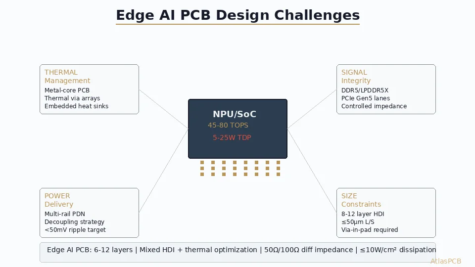
Edge AI PCB design requires solving three simultaneous challenges: delivering 15–50W to NPU/accelerator chips with < 5% voltage droop under 100A/μs transients, dissipating 2–5 W/cm² from compact packages without fans, and routing LPDDR5X at 8.5 Gbps with tight length matching on 8–12 layer HDI stackups. Success depends on co-designing the power delivery network, thermal via arrays, and signal routing as an integrated system rather than sequential design steps.
The Inference Flip: Why Edge AI PCB Design Is Different
By mid-2026, inference workloads account for approximately two-thirds of all AI compute, surpassing training for the first time. This “inference flip” has moved AI processing from distant data centers to edge devices — cameras, robots, medical instruments, autonomous vehicles, and industrial controllers.
For PCB designers, this shift creates a new class of design challenge. Cloud AI uses massive server boards with unlimited power and cooling budgets. Edge AI demands the same computational density in thermally constrained, battery-powered, or passively cooled form factors.
The economics drive this trend: cloud inference costs become unsustainable when devices process data continuously. A single AI camera running cloud inference costs $50–100/month in API fees. The same camera with an on-device NPU has near-zero marginal inference cost after the hardware investment.
This guide covers the PCB-level design techniques that make reliable edge AI hardware possible.
Power Delivery for NPU Processors
The Transient Challenge
Edge AI processors operate in two fundamentally different power states:
- Idle/standby: 1–5W, minimal current draw
- Full inference: 15–50W, peak current in microseconds
The transition between states happens in 1–10 μs — far faster than any DC-DC converter can respond. During this transient, only the PCB’s decoupling capacitor network and plane capacitance supply the surge current.
PDN Impedance Target
The target PDN impedance is:
Z_target = Vcore × ripple_tolerance / I_transient
For a typical edge AI processor:
- Vcore = 0.85V
- Ripple tolerance = ±3% (25.5 mV)
- I_transient = 20A step in 1 μs
Z_target = 0.0255 / 20 = 1.275 mΩ from DC to 100 MHz
This is an extraordinarily low impedance requirement that demands careful PCB design.
Decoupling Strategy
Bulk capacitors (DC–1 MHz):
- 4–8× 100 μF polymer tantalum or MLCC banks
- Placed within 15 mm of NPU package
- Provide charge during converter response time
Mid-frequency (1–30 MHz):
- 20–40× 1 μF 0201/0402 MLCC (X5R, 0.85V rated)
- Placed within 3 mm of BGA escape vias
- Critical frequency range for most transients
High-frequency (30–500 MHz):
- 10–20× 100 nF 0201 MLCC
- Placed on same layer as NPU pads or via-connected on adjacent layer
- Mounting inductance must be < 200 pH (requires via-in-pad)
Plane capacitance (>500 MHz):
- 2 oz copper power/ground plane pair with thin dielectric (2–3 mil)
- Provides 500–1000 pF per square inch
- Zero ESL — responds instantaneously to multi-GHz noise
Layout Rules for Edge AI PDN
- Dedicate 2+ plane layers to NPU power/ground — do not route signals through power islands
- Via-in-pad for all decoupling capacitors — eliminates trace inductance
- Star-point ground connection from NPU ground balls to ground plane
- Separate analog and digital power domains — NPU’s analog PLL supply needs ≤ 5 mV ripple
- Wide power traces for routing between VRM and BGA field: minimum 0.5 mm for each ampere of DC current
Thermal Management: The PCB as Heat Sink
Thermal Budget Analysis
For a fanless edge AI device with 25W TDP:
- Junction-to-case: 0.5°C/W (package thermal resistance)
- Case-to-ambient target: < 2.0°C/W (for Tj_max = 105°C at Ta = 45°C)
- PCB thermal contribution: 0.5–1.0°C/W from thermal via array
Thermal Via Array Design
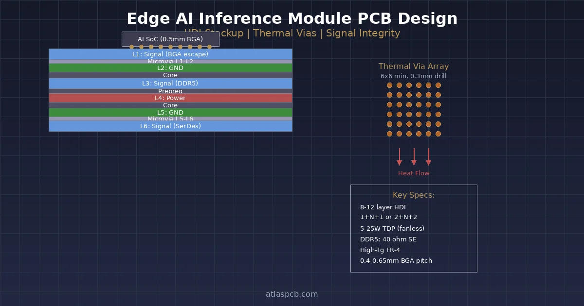
The thermal via array beneath the NPU’s thermal pad provides a low-resistance path from top copper to bottom copper (or to an embedded heat spreader):
Design parameters:
- Via diameter: 0.3 mm (standard drill, reliable plating)
- Via pitch: 0.6 mm (minimum for mechanical drill)
- Array size: matches thermal pad (typically 8×8 to 12×12)
- Plating: 25 μm copper wall (standard electrolytic)
- Fill: Copper-filled preferred (3× better conductivity than hollow)
Thermal conductivity calculation:
- Single via (0.3 mm dia, 25 μm wall, 1.6 mm board): R_th ≈ 120°C/W
- 64-via array (8×8): R_th ≈ 1.9°C/W
- Copper-filled 64-via array: R_th ≈ 0.8°C/W
Copper Coin / Embedded Heat Spreader
For designs exceeding 35W in fanless operation, thermal vias alone are insufficient. Embedded copper coins provide:
- Direct copper path from die to board bottom (R_th < 0.3°C/W)
- 2–3 mm thick copper slug pressed into PCB cavity during lamination
- Enables bottom-side heatsink attachment with thermal interface material
Manufacturing considerations:
- Copper coin must match PCB thickness ±0.05 mm
- Cavity routing after inner layer imaging
- Coin insertion before final lamination press
- Typical cost adder: +$5–15 per board (volume dependent)
Lateral Heat Spreading
Don’t neglect lateral conduction through copper planes:
- 2 oz copper plane: spreads heat effectively within 15 mm radius
- 4 oz copper (specialty): doubles spreading radius, enables plane-based heatsinking
- Component-free keepout zone around NPU: allows heat to spread before hitting adjacent ICs
Edge AI PCB Manufacturing
AtlasPCB manufactures 8–16 layer HDI boards with copper-filled thermal vias, embedded coins, and impedance-controlled stackups for AI edge devices.
View AI Hardware Capabilities →LPDDR5X Routing: 8.5 Gbps on a Budget
Why LPDDR5X for Edge AI
Edge AI processors pair with LPDDR5X memory for:
- 8.5 Gbps/pin data rate (sufficient for transformer model inference)
- 50% lower power than DDR5 at equivalent bandwidth
- Package-on-Package (PoP) or discrete options
- x16/x32 channels matching NPU memory controllers
Routing Constraints
LPDDR5X routing at 8.5 Gbps requires:
- Length matching: ±0.5 mm within each byte lane (DQ to DQS)
- Impedance: 40–50 Ω single-ended, 80–100 Ω differential (per JEDEC)
- Trace width: 3–4 mil on FR-4 (depends on stackup)
- Spacing: ≥ 2× trace width to adjacent signals (crosstalk budget)
- Via stubs: Maximum 5 mil stub length (back-drilling or blind vias required)
- Reference plane continuity: No splits or voids beneath LPDDR routing
Stackup for LPDDR5X
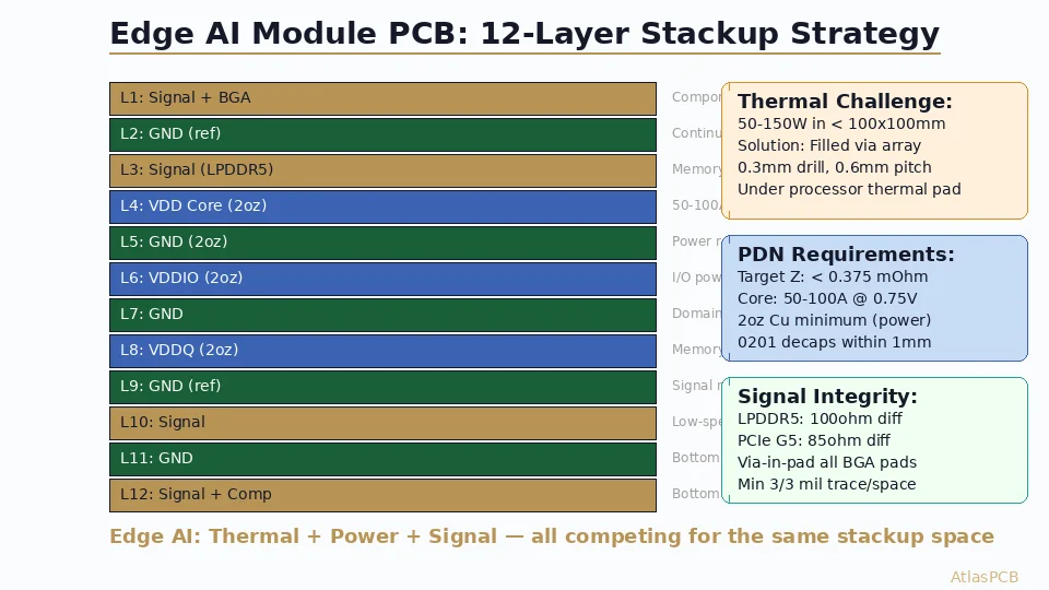
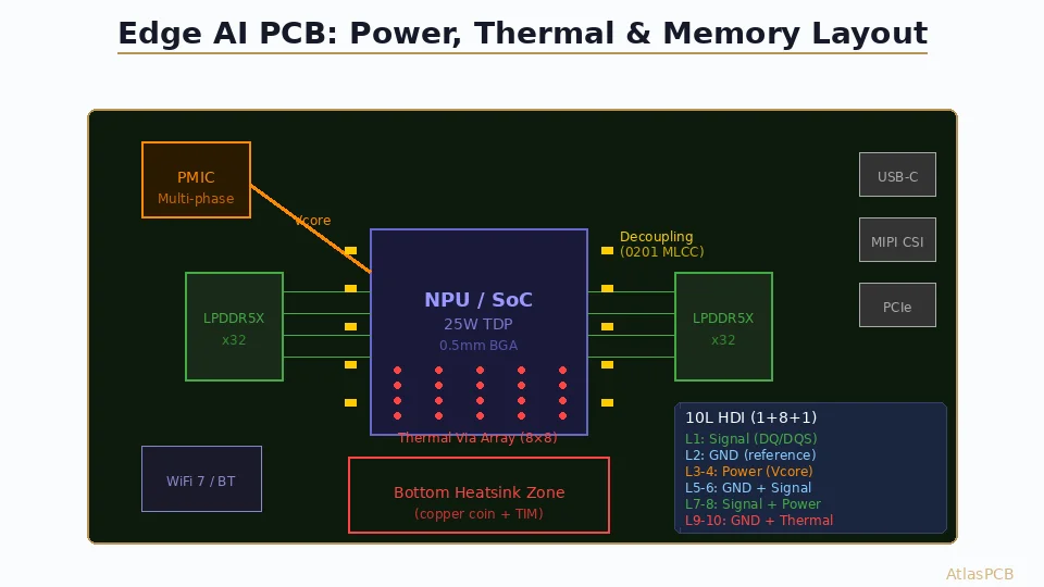
A typical 10-layer edge AI stackup optimized for LPDDR5X:
Layer 1:  Signal (LPDDR5X DQ/DQS + NPU BGA escape)
Layer 2:  Ground (continuous reference for L1)
Layer 3:  Signal (secondary routing, I2C, SPI, GPIO)
Layer 4:  Power (NPU Vcore)
Layer 5:  Ground (shielding between power and signal)
Layer 6:  Power (LPDDR VDDQ, 1.05V)
Layer 7:  Signal (LPDDR address/command)
Layer 8:  Ground (reference for L7, L9)
Layer 9:  Signal (high-speed interfaces: PCIe, USB, MIPI)
Layer 10: Ground/Power (mixed, with thermal via landing)
Routing Best Practices
- Route DQ/DQS on surface layer — shortest path, best impedance control
- Keep all byte lane signals on same layer — avoids via-induced skew
- Use ground-referenced stripline for address/command — better noise immunity
- Avoid crossing power plane splits — route around or use stitching capacitors
- Match via count per signal group — each via adds ~30 ps delay
HDI Stackup Strategies for Edge AI
Why HDI is Essential
Edge AI devices demand HDI because:
- NPU BGA pitch: 0.4–0.5 mm (requires microvias for escape)
- Board size constrained (wearable, camera module, drone)
- Layer count must be minimized for cost (every layer adds $)
- Blind/buried vias enable routing density without added layers
Build-Up Options
1+N+1 (one build-up per side):
- Cost-effective for 0.5 mm pitch BGA
- Microvia: 0.1 mm laser drill, aspect ratio ≤ 0.8:1
- Sufficient for most 8-layer edge AI designs
- 15–20% cost premium over standard through-hole PCB
2+N+2 (two build-ups per side):
- Required for 0.4 mm pitch or double-escape BGA
- Stacked microvias (via-on-via) for vertical routing
- Enables 10-layer board in 8-layer mechanical stack
- 30–40% cost premium
Any-Layer HDI:
- Maximum density, all vias are laser-drilled
- Required for 0.3 mm pitch (advanced mobile processors)
- Enables 6-layer board with density of 12-layer conventional
- 60–100% cost premium, limited manufacturer capability
Microvia Reliability for AI Hardware
Edge AI devices in industrial/automotive environments must pass:
- IPC-6012 Class 3 (2000+ thermal cycles)
- Automotive AEC-Q104 qualification
- IST (Interconnect Stress Test) per IPC-TM-650
Critical microvia rules:
- Stacked microvias: maximum 2 levels without reliability concern
- 3-level stacks: require copper-filled vias and specific plating chemistry
- Aspect ratio: ≤ 1:1 for laser vias (0.1 mm via in 0.1 mm dielectric)
- Target thickness fill: > 70% copper fill for reliable stacking
Component Selection Impact on PCB Design
NPU Package Formats
Current edge AI processors come in several packages affecting PCB design:
| Processor | Package | Pitch | Power | Layers Needed |
|---|---|---|---|---|
| Qualcomm QCS8550 | FC-BGA 17×17 | 0.5 mm | 15W | 8 (1+6+1) |
| NVIDIA Jetson Orin NX | 260-pin module | N/A* | 25W | 6–8 (carrier) |
| MediaTek Genio 1200 | FC-BGA 14×14 | 0.5 mm | 12W | 8 (1+6+1) |
| Hailo-15H | FC-BGA 13×13 | 0.5 mm | 8W | 6–8 |
| Intel Meteor Lake | Various | 0.4–0.5 mm | 35W | 10–12 (2+N+2) |
*Module-based designs shift complexity from customer PCB to module substrate
Memory Topology Impact
Edge AI memory architecture affects PCB complexity:
Package-on-Package (PoP):
- Memory stacked directly on NPU
- Eliminates long PCB traces
- PCB only needs power/ground connections to memory
- Simplifies routing significantly
Discrete LPDDR:
- Memory IC placed adjacent to NPU
- Requires full fly-by or T-branch routing
- Higher layer count but enables more memory capacity
- Used in industrial AI boxes (16–32 GB)
On-Package Memory (HBM2E for edge):
- Emerging in high-end edge (autonomous vehicles)
- No PCB-level memory routing required
- Substrate-level design (manufacturer handles)
Power Management IC (PMIC) Integration
Multi-Rail Architecture
A typical edge AI power tree:
- NPU Core: 0.75–0.85V @ 20A (dynamic voltage scaling)
- NPU I/O: 1.8V @ 2A
- LPDDR5X VDDQ: 1.05V @ 3A
- LPDDR5X VDD2: 1.8V @ 1A
- Connectivity (WiFi/BT/5G): 3.3V @ 0.5A, 1.2V @ 1A
- Sensor interfaces: 1.8V/3.3V @ 0.2A each
PMIC Placement Strategy
- PMIC within 10 mm of NPU — minimizes trace length for Vcore
- Inductor placement: Between PMIC and NPU, minimal loop area
- Input capacitor bank: Adjacent to PMIC input pins
- Feedback divider: Close to PMIC FB pin, away from switching node
- Sense lines: Kelvin-connected to NPU power pads, not PMIC output
Layout Rules for Multi-Phase Converters
High-current NPU rails use multi-phase buck converters:
- Phase interleaving: Reduces input/output ripple by N× (N = phase count)
- Symmetric layout: Each phase must have identical trace length and loop area
- Current sharing: Mismatch in parasitic resistance causes unequal phase currents
- Thermal balance: Spread phases around the NPU to distribute heat
EMC Considerations for Edge AI
Switching Noise from DC-DC
Multi-phase buck converters switching at 500 kHz–2 MHz generate significant EMI:
- Conducted: Through power planes to other circuits
- Radiated: From inductor magnetic fields and switch node ringing
Mitigation:
- Shield inductors (closed magnetic circuit) — 20 dB radiated reduction
- Boot resistor on high-side FET — reduces dV/dt and ringing
- Snubber circuits on switch nodes — damps parasitic oscillation
- Ground plane continuous beneath converter — contains return currents
NPU Clock Harmonics
Edge AI processors have internal clocks up to 2 GHz with harmonics extending to 10+ GHz:
- Via fencing around NPU BGA area contains emissions
- Ground plane unbroken beneath package
- 3W (3× trace width) spacing from NPU signals to board edge
- Consider EMI shield can for regulatory compliance
Design Validation and Testing
Pre-Production Simulation
Before committing to fabrication:
- PDN simulation: Target impedance flat ±10% from DC to 500 MHz
- Thermal simulation: Verify Tj < 95°C at worst-case ambient and workload
- Signal integrity: Eye diagram > 60% open at receiver for LPDDR5X
- EMC pre-scan: Identify potential radiation sources and add mitigation
Production Testing
- In-circuit test: Verify power rail voltages, decoupling capacitor values
- Functional test: Boot and run inference benchmark (confirms signal integrity)
- Thermal characterization: IR camera mapping under sustained inference workload
- Accelerated life test: Temperature cycling per target environment class
Further Reading
- AI Hardware PCB Thermal Management and Multilayer Design
- PCB Power Integrity and Decoupling Design
- HDI PCB Stackup Design: Advanced Techniques
- Controlled Impedance PCB: Stackup Calculations Guide
- PCB Thermal Via Array Design Rules
Designing PCBs for edge AI products? AtlasPCB specializes in HDI manufacturing for AI hardware — copper-filled microvias, impedance-controlled stackups, and embedded thermal solutions. From prototype to production, we build the boards that make on-device AI work. Get a quote for your AI hardware project.
About AtlasPCB — We specialize in complex PCB manufacturing for HDI, RF, and high-reliability applications. Explore our HDI PCB manufacturing capabilities, or get an aluminum and metal-core PCB services . Every order includes free engineering review. Get your quote.
Reviewed by AtlasPCB Engineering Team — IPC-certified manufacturing specialists with 15+ years of production experience in HDI, RF, and high-reliability PCB fabrication. Content based on factory floor data and real customer design reviews.
Frequently Asked Questions
What layer count is typical for edge AI PCBs in 2026?
How do you manage thermal dissipation on fanless edge AI devices?
What is the biggest PCB design mistake in edge AI products?
- edge AI
- NPU
- PCB design
- power delivery
- thermal management
- LPDDR5X
- HDI
- inference hardware