· Thomas Webb · Engineering · 7 min read
Glass Core Substrates for AI Packaging
Intel's high-volume glass substrate manufacturing for Xeon 6+ processors signals a paradigm shift from organic ABF substrates. Understand the implications for PCB fabricators, material suppliers, and AI hardware designers.
Quick Answer
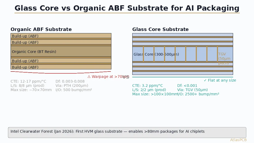
Glass core substrates replace organic ABF (Ajinomoto Build-up Film) materials with glass panels that match silicon's thermal expansion coefficient (CTE ~3 ppm/°C vs. organic's 12-17 ppm/°C). Intel's January 2026 production launch of Clearwater Forest on glass substrates demonstrated 50% higher interconnect density, eliminated warpage at large package sizes, and enabled the chiplet architectures that next-generation AI accelerators require. This technology fundamentally shifts PCB substrate manufacturing from lamination-based chemistry to semiconductor-adjacent lithography.
The Organic Substrate Wall
For two decades, Ajinomoto Build-up Film (ABF) substrates have been the foundation of advanced semiconductor packaging. The laminate-based approach — layer upon layer of resin-coated copper foil, mechanically drilled and chemically etched — scaled elegantly from flip-chip packages to today’s complex multi-die architectures.
But organic substrates have hit a physics wall. As AI accelerators grew larger and more power-dense, three fundamental limitations emerged:
Warpage: Organic materials (CTE 12-17 ppm/°C) expand and contract differently than silicon (CTE 3.1 ppm/°C). At package sizes above 70×70mm, this CTE mismatch creates warpage that prevents reliable flip-chip bonding.
Interconnect density: Standard ABF processes achieve minimum line/space of 8/8 µm in production. AI chiplet architectures require 2/2 µm for die-to-die communication — a 4× density gap.
Signal integrity: At 224G PAM4 signaling speeds emerging in next-generation AI networks, organic dielectric loss tangent (Df 0.003-0.008) becomes a bandwidth limiter. Glass offers Df <0.001 across relevant frequencies.
Intel’s decision to bring glass substrates into high-volume manufacturing for Clearwater Forest wasn’t incremental improvement — it was an acknowledgment that organic substrates cannot support the AI hardware roadmap beyond current generation.
Intel Clearwater Forest: First HVM Glass Substrate Product
Announced at CES 2026 and entering production in January 2026, Intel’s Xeon 6+ “Clearwater Forest” processor represents the first commercial IC product fabricated on glass core substrates at high volume.
Technical Specifications
- Die: Multiple chiplets on Intel 18A process
- Package size: >80mm × 80mm (beyond organic warpage limit)
- Substrate: Glass core with build-up redistribution layers
- Interconnect: Through-Glass Vias (TGV) at 50µm pitch
- Line/space: 2/2 µm (vs. 8/8 µm on latest organic ABF)
- Layers: 10+ redistribution layers on glass core
- CTE match: Glass core 3.2 ppm/°C vs. silicon 3.1 ppm/°C
Performance Benefits Demonstrated
| Parameter | Organic ABF (Sapphire Rapids) | Glass Core (Clearwater Forest) |
|---|---|---|
| Maximum package size | 70×70mm (warpage-limited) | >100×100mm (no practical limit) |
| I/O density | 500 bump/mm² | 2,500+ bump/mm² |
| Power delivery resistance | 1.0 mΩ typical | 0.4 mΩ typical |
| Signal loss at 56 GHz | -2.5 dB/cm | -0.8 dB/cm |
| Warpage at reflow | 100-300 µm | <30 µm |
| Die-to-die bandwidth | 16 Tbps (limited by pitch) | 40+ Tbps |
How Glass Substrates Are Made
Glass substrate manufacturing is fundamentally different from organic PCB fabrication:
Step 1: Glass Panel Preparation
- Starting material: High-purity glass panels (Gen 3.5 display glass or specialty borosilicate)
- Thickness: 300-500 µm (vs. 60-100 µm for ABF core)
- CTE engineered via composition: adjustable from 3-8 ppm/°C
- Surface preparation: Chemical mechanical polish (CMP) to <1nm roughness
Step 2: Through-Glass Via (TGV) Formation
- Laser-induced deep etching: Ultrafast laser creates modification tracks
- Chemical etch: HF-based wet etch selectively removes laser-modified glass
- Result: Vias at 30-50 µm pitch (vs. 200-300 µm for organic PTH)
- Aspect ratio: Up to 20:1 achievable
Step 3: Metallization
- Seed layer: PVD sputtered TiW/Cu (vs. electroless Cu for organic)
- Pattern plating: Semi-additive process (SAP) at 2/2 µm L/S
- Via fill: Electroplated copper fills TGVs from bottom-up
- Planarization: CMP produces atomically flat surface for next layer
Step 4: Build-Up Layers
- Dielectric: Photo-definable polyimide or inorganic SiO₂ (vs. ABF resin)
- Layer count: 6-12 redistribution layers built on each side of glass core
- Registration: Lithographic alignment <±1 µm (vs. ±10 µm for organic lamination)
Step 5: Bumping and Singulation
- UBM (Under-Bump Metallurgy): Sputtered multi-layer for flip-chip or micro-bump
- Singulation: Laser or mechanical dicing of glass panel into individual substrates
- Final test: Electrical probing of all interconnects
Advanced Substrate Capabilities
High-Density Interconnect for AI Hardware
While glass substrates are in the semiconductor domain, AtlasPCB supports the PCB ecosystem surrounding AI packages — motherboards, interposers, and high-speed interconnect boards designed to interface with next-generation processors.
Explore Our HDI Capabilities →Why Glass Matters for AI Specifically
The connection between glass substrates and AI hardware is direct and structural:
Power Delivery
AI accelerators consume 500-1000W per package. Power must be delivered through the substrate with minimal resistance to avoid voltage droop during transient workloads. Glass substrates enable:
- Thicker, wider redistribution layer traces (lower resistance)
- More power/ground via columns (lower inductance)
- Better planarity = more uniform bump contact = lower contact resistance
The cumulative effect: 40-60% reduction in package-level power delivery impedance, which translates directly to higher clock frequencies and wider voltage margins.
Chiplet Architecture Support
Modern AI processors (NVIDIA Blackwell, AMD MI400, Intel Clearwater Forest) use multi-chiplet designs where 4-12 compute dies communicate on a shared substrate. These die-to-die links require:
- Extremely fine pitch (36-55µm bump pitch between chiplets)
- Very flat substrate (warpage <30µm for reliable thermocompression bonding)
- Low-loss interconnect (die-to-die links at 16-32 Gbps per lane)
Organic substrates cannot maintain flatness at the package sizes these multi-chiplet designs require. Glass solves this geometrically — matching silicon’s thermal expansion eliminates the warpage that prevents scaling.
Bandwidth Density
AI training workloads are memory-bandwidth-limited. HBM4 memory stacks communicate with the processor through thousands of parallel lanes at 8-16 Gbps each. The substrate interconnect density directly limits how much memory bandwidth can reach the compute die:
- Organic: ~500 connections/mm² → limited to 4-6 HBM stacks
- Glass: ~2,500 connections/mm² → supports 8-12+ HBM stacks per package
More HBM stacks per package = more memory bandwidth = faster training. Glass substrates are literally a prerequisite for next-generation AI training hardware performance scaling.
The Competitive Landscape
Intel: First Mover Advantage
Intel’s glass substrate program (announced 2023, HVM 2026) gives them a 2-3 year lead over competitors:
- Proprietary TGV formation process
- Integrated panel-level manufacturing in their Advanced Packaging facility
- Clearwater Forest proves production viability — no longer a research project
Chinese Players Racing to Catch Up
As reported by ETNews and IC&PCB Union, Chinese companies are accelerating glass substrate investment:
Visionox: Display maker pivoting to glass substrates, leveraging existing glass handling and lithography expertise. RMB 5 billion investment program announced for 2026, targeting both display and semiconductor substrate applications.
AKM Meadville: Leading Chinese HDI substrate supplier has established a prototype glass substrate pilot line. Their existing dominance in organic IC substrates provides the customer relationships needed to transition designs to glass.
WG Tech / TGV Tech: Subsidiary focused exclusively on Through-Glass Via technology. Already delivering small-batch glass substrates for 1.6T optical modules — an early commercial application outside of compute.
Korean Push
South Korea is racing to close the packaging gap with Taiwan and China. Samsung’s foundry division and Korean substrate makers (Samsung Electro-Mechanics, LG Innotek) are investing in glass substrate R&D to support Samsung’s own AI accelerator packaging roadmap.
Impact on the PCB Industry
What Changes for PCB Fabricators
Glass substrates don’t replace PCBs — they replace the IC substrate layer between the chip and the PCB. The implications:
Motherboard design changes: Glass substrate packages have different ball patterns, power delivery requirements, and thermal interfaces. PCB motherboards must be redesigned for each glass-substrate processor generation.
Signal integrity requirements increase: With the package-level interconnect no longer the bottleneck, the PCB motherboard traces become the limiting factor. Expect tighter impedance tolerances (±5% standard) and ultra-low-loss material adoption on PCB motherboards.
Power delivery copper weight: Glass substrates enable higher processor power (>600W TDP). PCB power planes must scale proportionally — 4-8 oz copper, embedded bus bars.
IC substrate market disruption: Traditional ABF substrate fabricators (Ibiden, Shinko, Unimicron) must either invest in glass capabilities or risk market share erosion to glass-native manufacturers.
What Stays the Same
- PCBs still connect everything at the system level
- Increasing PCB complexity supports glass substrate packages
- High-layer-count, controlled-impedance PCB demand actually increases
- Fabricators serving AI server markets see demand growth regardless of substrate technology choice
Timeline: Glass Substrate Adoption Roadmap
| Timeframe | Application | Volume |
|---|---|---|
| 2026 (now) | Intel Xeon 6+ server CPUs | Thousands/month |
| 2027 | NVIDIA AI accelerators (rumored) | Tens of thousands/month |
| 2028 | AMD data center CPUs + AI GPUs | Hundreds of thousands/month |
| 2029 | High-end networking ASICs (800G+) | Millions/year |
| 2030+ | 5G/6G RF modules, automotive radar | Mass market penetration |
The transition from organic to glass substrates will take a decade to fully play out — but for AI hardware designers, it’s happening now.
What Hardware Engineers Should Do Today
- Monitor package ball maps: Next-generation processors will have different substrate ball pitches — plan PCB footprint libraries accordingly
- Specify ultra-low-loss PCB materials: Megtron 6/7, Tachyon, or equivalent for signals interfacing with glass-substrate processors
- Design for higher power: Plan thermal solutions for >600W packages
- Engage your PCB fabricator early: Discuss advanced material availability and controlled impedance capabilities for AI server boards
Further Reading
- HDI PCB Stackup Design Guide
- TSMC CoWoS 11× Capacity Growth: Reshaping PCB Substrate Technology
- Controlled Impedance PCB Stackup Design Rules
- PCB Via-in-Pad Plated Over (VIPPO) Guide
Building PCB systems for next-generation AI processors? Talk to our engineering team about motherboard design for glass-substrate packages. We’ll help you select materials, validate impedance, and optimize power delivery for the most demanding AI hardware platforms.
About AtlasPCB — We specialize in complex PCB manufacturing for HDI, RF, and high-reliability applications. Explore our full PCB manufacturing capabilities, or get an instant online quote . Every order includes free engineering review. Get your quote.
Reviewed by AtlasPCB Engineering Team — IPC-certified manufacturing specialists with 15+ years of production experience in HDI, RF, and high-reliability PCB fabrication. Content based on factory floor data and real customer design reviews.
Frequently Asked Questions
Why can't organic substrates support next-generation AI chips?
What manufacturing changes do glass substrates require versus organic?
When will glass substrates affect mainstream PCB manufacturing?
- glass-substrate
- ai-packaging
- intel
- advanced-packaging
- pcb-substrate
- cowos