· AtlasPCB Engineering · Engineering · 9 min read
HDI PCB Manufacturer Pricing: Sequential Lamination vs Any-Layer — What Each Extra Cycle Actually Costs
HDI PCB pricing is opaque because manufacturers rarely explain WHY each sequential lamination cycle adds 40-60% to cost. This breakdown reveals the actual cost drivers — from laser drilling to alignment registration — and shows when any-layer construction becomes cheaper per-via than conventional sequential HDI.
Quick Answer
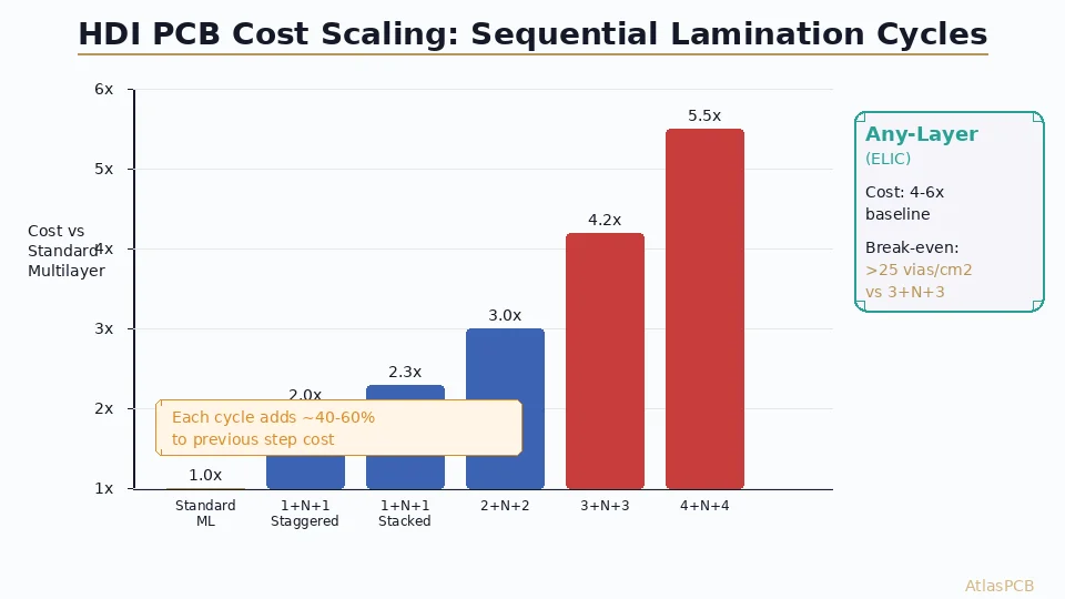
Each sequential lamination cycle in HDI fabrication adds approximately 40-60% to base board cost — not because of material, but because of added laser drilling passes, lamination cycles, and cumulative registration alignment challenges. At 3+N+3 complexity (6 sequential lamination cycles total), any-layer (ELIC) construction often becomes cost-competitive because it uses a single standardized process flow regardless of layer count. The crossover point depends on via density: above 25-30 microvias per square centimeter, any-layer beats sequential on cost-per-connection.
The 30-Second Decision
| HDI Type | Typical Cost vs Standard ML | Best For | Avoid When |
|---|---|---|---|
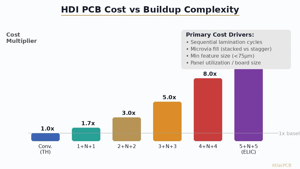
| 1+N+1 (staggered) | 1.8-2.2x | Standard BGA breakout, moderate density | Density fits on standard vias |
| 1+N+1 (stacked, filled) | 2.0-2.5x | Via-in-pad for fine-pitch BGA | Staggered would work |
| 2+N+2 | 2.5-3.5x | 0.4-0.5mm pitch BGA, high-speed memory | Can redesign with creative routing |
| 3+N+3 | 3.5-5.0x | 0.3mm pitch, extreme density | Consider any-layer instead |
| Any-layer (ELIC) | 4.0-6.0x | Maximum density, all-layer connectivity | Low via density (sequential cheaper) |
Why Each Lamination Cycle Costs What It Does
The pricing of HDI PCBs mystifies many hardware engineers because the cost scaling isn’t proportional to material addition. Adding two thin buildup layers (which add perhaps $2-3 in raw material to a 100x100mm board) somehow increases price by $50-150 per piece at prototype quantity. Understanding where that cost actually goes reveals optimization opportunities.
Each sequential lamination cycle requires five distinct process steps that standard multilayer fabrication doesn’t: laser via drilling (separate program, separate pass for each buildup layer), desmear/seed (preparing blind via walls for plating), electrolytic copper fill or flash (plating the vias), surface preparation for next lamination (oxide treatment or alternative), and precision alignment lamination with registration verification. Each of these steps has equipment time cost, chemistry cost, and — critically — yield risk.
In our production facility, we track cycle time per sequential lamination step. A standard 8-layer through-hole board goes through ONE lamination cycle (total pressing), ONE drilling pass, and ONE plating sequence. An 8-layer 2+N+2 HDI board with the same layer count requires FIVE lamination cycles, THREE drilling passes (two laser, one mechanical), and THREE plating sequences. The raw processing time is approximately 3.2x longer, which directly maps to the 2.5-3.5x price multiplier after accounting for material costs and yield loss.
HDI COST OPTIMIZATION
Can Your Design Be Built at Lower HDI Complexity?
Send your BGA assignments and routing constraints. Our HDI team evaluates whether a simpler buildup achieves your density requirements — often saving 30-40% on PCB cost.
Submit for Analysis ›
Sequential Lamination Cost Breakdown: Where the Money Goes
Breaking down the cost of a single sequential lamination cycle reveals five distinct cost buckets. Understanding these individually helps engineers evaluate which HDI complexity level actually aligns with their technical requirements versus which represents unnecessary gold-plating.
Laser Drilling (25-35% of cycle cost): Each buildup layer requires its own UV or CO2 laser drilling pass. At typical volumes (100-500 pieces), laser drilling costs $0.002-0.005 per via depending on diameter and depth. A moderately complex HDI layer with 2000-5000 microvias per board adds $4-25 in laser drilling cost per piece. This scales linearly with via count — so a design with 500 microvias per layer costs significantly less than one with 5000. Optimizing via count through better routing directly reduces laser drilling cost.
Copper Fill/Plating (20-25% of cycle cost): Filled microvias (required for stacked via structures and via-in-pad) require electrolytic copper filling to achieve planar surface. This process is slower than standard flash plating, requires specialized chemistry with proprietary additives, and has tighter process windows (voids = rejects). Staggered microvias requiring only flash plating cost approximately 40% less than filled vias for this step.
Lamination Alignment (15-20% of cycle cost): Each sequential lamination must register to the previous layers with accuracy better than ±25 microns for standard HDI (±15 microns for advanced). This requires X-ray alignment systems, precision tooling, and slower press cycles with controlled temperature ramp rates. Registration accuracy degrades with each additional cycle, which is why 4+N+4 and 5+N+5 boards require heroic manufacturing measures.
Yield Loss Allocation (15-20% of cycle cost): This is the hidden cost driver. Each sequential lamination cycle introduces new defect opportunities: microvia voids, delamination at prior layer interfaces, and registration drift. In our production, typical yield per cycle is 95-97% for experienced HDI shops. Compounded across cycles: 1+N+1 = 90-94% cumulative, 2+N+2 = 86-91%, 3+N+3 = 81-88%. The manufacturer prices boards to account for expected scrap — so a 3+N+3 board includes approximately 15-20% scrap cost in the unit price.
Inspection and Testing (10-15% of cycle cost): Each completed lamination cycle requires inspection before proceeding — typically automated optical inspection (AOI) of the patterned layer, and sometimes X-ray verification of via fill quality. You can’t rework a bad microvia after the next layer is laminated on top of it, so these inspections gate whether the panel continues in production or gets scrapped.
Any-Layer HDI: When the Fixed Process Wins on Economics
Any-layer construction (ELIC — Every Layer Interconnect) takes a counter-intuitive approach to cost optimization: instead of building outward from a core with sequential additions, it builds ALL layers sequentially using the same process flow. Every dielectric is a buildup; every via is a laser-drilled, copper-filled microvia; every layer connects to every other layer through stacked via pillars.
This sounds more expensive — and for simple designs, it is. But at high complexity levels (3+N+3 and above), any-layer achieves cost parity or even advantages because the process is completely standardized. The same laser drilling program, plating recipe, and lamination parameters apply to every layer. There’s no mixing of mechanical drills with laser vias, no core-layer processing different from buildup-layer processing. This standardization improves yield and reduces setup complexity.
The crossover point where any-layer becomes cost-competitive depends primarily on via density. Our production data shows the transition occurs at approximately 25-30 microvias per square centimeter of board area when comparing against 3+N+3 sequential construction. Below this density, sequential lamination is cheaper because the simpler 1+N+1 or 2+N+2 structures suffice. Above this density, any-layer’s yield advantage (consistent process) and its elimination of through-hole drilling (which becomes the bottleneck at extreme density) make it the economical choice.
For smartphone-class designs (0.3mm pitch BGA, 50+ microvias/cm2), any-layer is definitively cheaper than achieving the same connectivity with sequential construction. For industrial/automotive HDI (0.5mm pitch, 10-15 microvias/cm2), sequential 1+N+1 or 2+N+2 remains the cost-optimal approach.
ADVANCED HDI CAPABILITY
Up to 5+N+5 HDI with Stacked Microvias
Sequential lamination and any-layer builds with 75um laser vias. We handle the complexity — you get first-article yield above 90%.
Cost Optimization Strategies That Actually Work
Hardware engineers often accept the first HDI quote without questioning whether the specified buildup is truly necessary. In our experience reviewing incoming designs, approximately 30-40% of boards specified as 2+N+2 can be redesigned as 1+N+1 with creative routing strategies — saving 30-40% on PCB cost without compromising electrical performance.
Strategy 1: Route on core layers aggressively. The core layers in an HDI stackup use standard through-hole vias (cheap) and don’t require sequential lamination. Every signal that can route on core layers instead of buildup layers reduces the number of microvias needed and potentially reduces the required buildup complexity. Before accepting that you need 2+N+2, verify that your core layers are fully utilized for routing.
Strategy 2: Use staggered microvias instead of stacked where possible. Stacked microvias require copper filling (expensive) and tighter registration (higher yield loss). Staggered microvias only need flash plating and have relaxed registration requirements. The trade-off is larger pad diameter (staggered needs offset landing pads), which consumes more routing area. But for 0.5mm+ pitch BGAs, staggered vias deliver the same connectivity at 60-70% the via processing cost.
Strategy 3: Evaluate whether HDI is actually required. A surprising number of designs specified as HDI can be built using mechanical blind vias (0.15mm minimum diameter) combined with via-in-pad processing on standard sequential multilayer construction. This hybrid approach — mechanical blind vias where space allows, standard through-vias elsewhere — often costs 30-50% less than laser-drilled HDI while achieving adequate BGA breakout for 0.65mm+ pitch devices.
Strategy 4: Consolidate HDI to one side. Many designs have high-density components (fine-pitch BGA) on only one side of the board. Building asymmetric HDI (2+N+0 instead of 1+N+1) concentrates complexity on the side that needs it, saving one complete sequential lamination cycle. The trade-off is asymmetric board construction (potential bow/twist), which is manageable for boards under 100x100mm.
2026 Pricing Reality: What HDI Actually Costs at Different Volumes
For planning purposes, here’s what our current production pricing looks like across HDI complexity levels. These are approximate per-piece costs for a 100x100mm board, 10-layer total:
| HDI Type | 10 pieces | 100 pieces | 1000 pieces | Key Cost Driver |
|---|---|---|---|---|
| Standard 10L (through-hole) | $45-65 | $18-28 | $8-12 | Baseline |
| 10L, 1+N+1 staggered | $85-120 | $35-55 | $15-22 | 1 laser drill pass |
| 10L, 1+N+1 stacked/filled | $100-150 | $42-65 | $18-28 | Via fill process |
| 10L, 2+N+2 | $160-240 | $65-100 | $28-42 | 2 sequential cycles |
| 10L, 3+N+3 | $250-380 | $100-160 | $42-65 | 3 cycles, yield risk |
| 10L, any-layer | $300-450 | $120-180 | $48-72 | All-sequential build |
These prices reflect typical production at our facility with standard materials (IT-180A or equivalent, Tg 180C). Rogers or specialty laminates on HDI layers add 30-80% to material cost. Lead time scales similarly: standard 10L takes 10-12 working days; 1+N+1 adds 3-5 days; 2+N+2 adds 5-8 days; 3+N+3 adds 8-12 days.
The NRE component (tooling, laser programming, first-article setup) is relatively fixed at $200-500 regardless of quantity. This is why the per-piece cost drops dramatically from 10 to 100 pieces — NRE amortization dominates at small quantities.
ATLASPCB
Get Your HDI PCB Quoted — With Optimization Recommendations
Upload your Gerber and stackup. We'll quote your specified buildup AND suggest optimizations that could reduce cost by 20-40% without compromising performance.
Upload for Quote ›
Reviewed by AtlasPCB Engineering Team — 15+ years in advanced PCB fabrication for RF, HDI, and rigid-flex applications.
Related Reading:
About AtlasPCB — We specialize in complex PCB manufacturing for HDI, RF, and high-reliability applications. Explore our HDI PCB manufacturing capabilities, multilayer PCB fabrication up to 30 layers, or get an instant online PCB quote . Every order includes free engineering review. Get your quote.
Reviewed by AtlasPCB Engineering Team — IPC-certified manufacturing specialists with 15+ years of production experience in HDI, RF, and high-reliability PCB fabrication. Content based on factory floor data and real customer design reviews.
Frequently Asked Questions
How much does each sequential lamination cycle add to HDI PCB cost?
What is any-layer HDI and when is it cost-effective?
Why does HDI cost so much more than standard multilayer PCBs?
Can I reduce HDI cost by optimizing my buildup structure?
What is the minimum order quantity for HDI PCBs to get reasonable pricing?
- HDI PCB manufacturer
- multilayer PCB cost
- PCB stackup design guide
- sequential lamination
- any-layer HDI
- microvia