· David Okafor · Engineering · 6 min read
Sequential Lamination vs Build-Up HDI
Compare sequential lamination and SBU build-up processes for HDI PCBs. Learn when each approach delivers optimal density, reliability, and cost for your multilayer design.
Quick Answer
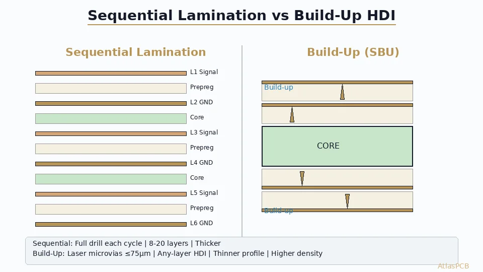
Sequential lamination builds a PCB by laminating and drilling one core-pair at a time (suitable for 8-20 layers with through-vias), while build-up (SBU) adds dielectric and copper layers sequentially with laser microvias (enabling any-layer HDI with ≤75 μm vias for maximum routing density in compact designs).
Understanding the Two Fundamental HDI Approaches
High-density interconnect (HDI) PCB manufacturing uses two fundamentally different process flows to achieve multilayer connectivity. The choice between sequential lamination and build-up (SBU — Sequential Build-Up) determines your design’s routing density, reliability profile, cost structure, and manufacturing lead time.
Sequential Lamination: The Traditional Approach
Process Overview
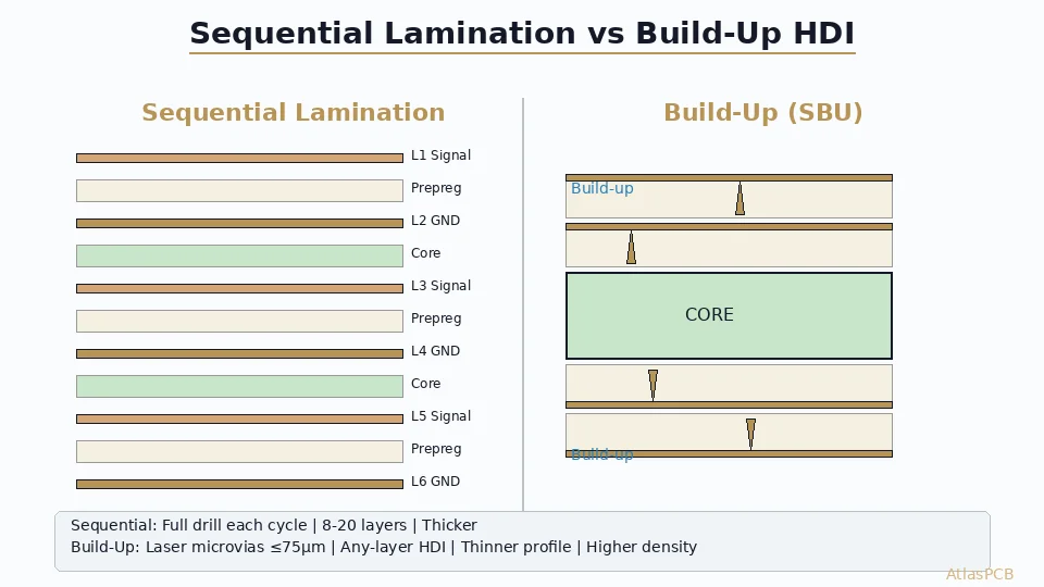
Sequential lamination builds a PCB by bonding pre-fabricated double-sided cores together with prepreg layers, drilling through-holes or blind vias at each stage:
- Core fabrication — Etch individual double-sided cores (typically 0.1-0.4 mm thick)
- First lamination — Bond 2-4 cores with prepreg; drill and plate through-vias
- Second lamination — Add outer cores; drill new through-vias connecting outer layers
- Repeat — Continue until all layers are integrated
- Final processing — Surface finish, solder mask, routing
When Sequential Lamination Excels
Sequential lamination remains the preferred choice for:
- High layer counts (16-40+ layers) — Backplanes, server boards, networking equipment
- Heavy copper requirements — Power planes at 2-4 oz copper weight
- Through-hole reliability — Applications requiring mechanical PTH connections
- Mixed technology — Boards combining HDI regions with standard-density areas
- Cost-sensitive high-layer designs — When microvia density isn’t needed on all layers
Design Constraints
| Parameter | Typical Capability |
|---|---|
| Minimum via drill | 0.15-0.2 mm (mechanical) |
| Via pad diameter | 0.35-0.45 mm |
| Layer-to-layer registration | ±50-75 μm |
| Minimum trace/space | 75/75 μm |
| Aspect ratio (through-via) | 10:1 to 12:1 |
| Buried via aspect ratio | 8:1 |
Build-Up (SBU) HDI: Maximum Density
Process Overview
Build-up technology starts from a central core and adds layers one at a time using dielectric film lamination and laser via drilling:
- Core preparation — Fabricate a conventional 2-4 layer core
- Dielectric application — Laminate RCC (Resin Coated Copper) or ABF film
- Laser drilling — CO₂ or UV laser creates microvias (50-100 μm diameter)
- Metallization — Desmear, electroless copper seed, electrolytic copper plating
- Pattern and etch — Define trace geometry on the new layer
- Repeat — Build additional layers (typically 1-5 per side)
The Any-Layer HDI Advantage
The most advanced form of build-up HDI — any-layer or ELIC (Every Layer Interconnect) — allows microvias to connect any adjacent layer pair without restrictions. This eliminates the traditional constraint where vias consume routing area on intermediate layers.
Density comparison:
| BGA Pitch | Sequential (escape layers) | Build-Up HDI (escape layers) |
|---|---|---|
| 1.0 mm | 2 layers | 1 layer |
| 0.8 mm | 3-4 layers | 1-2 layers |
| 0.65 mm | 5-6 layers (marginal) | 2-3 layers |
| 0.5 mm | Not feasible | 2-3 layers |
| 0.4 mm | Not feasible | 3-4 layers |
Design Capabilities
| Parameter | Standard Build-Up | Advanced Any-Layer |
|---|---|---|
| Microvia diameter | 75-100 μm | 50-75 μm |
| Via pad diameter | 150-200 μm | 120-150 μm |
| Layer registration | ±25-37 μm | ±15-25 μm |
| Min trace/space | 50/50 μm | 30/30 μm |
| Stacked via depth | 2-3 layers | 5+ layers (filled copper) |
| Dielectric thickness | 40-80 μm | 30-60 μm |
Struggling with BGA Breakout in Your HDI Design?
AtlasPCB manufactures both sequential and build-up HDI boards, with any-layer capability down to 50 μm microvias. Our DFM team reviews your design free of charge.
Submit Your HDI Design →Head-to-Head Comparison
Routing Density
Build-up HDI wins decisively on routing density per unit area:
- Via capture pad area: Build-up microvias use 0.02 mm² per connection vs 0.12 mm² for mechanical vias — a 6× improvement
- Fanout efficiency: A 625-pin BGA at 0.5 mm pitch requires 2 build-up layers vs being physically impossible with sequential lamination
- Trace density: 30/30 μm L/S in build-up vs 75/75 μm in sequential
Reliability
Both processes achieve high reliability when properly designed, but through different mechanisms:
Sequential lamination strengths:
- Through-hole vias survive 1000+ thermal cycles (-55°C to +125°C)
- Barrel crack resistance proportional to copper thickness (25+ μm typical)
- Proven qualification data spanning decades
Build-up HDI strengths:
- Filled and capped microvias eliminate trapped moisture/flux
- Shorter current paths reduce resistive heating
- Lower CTE mismatch (thinner dielectric layers = less Z-axis expansion)
- Stacked microvias with copper filling achieve >1000 cycle reliability per IPC-6012E
Caution with stacked microvias:
- Stacking more than 3 unfilled microvias significantly reduces reliability
- Always specify copper-filled microvias for stacks of 3+
- Target fill ratio >90% verified by cross-section
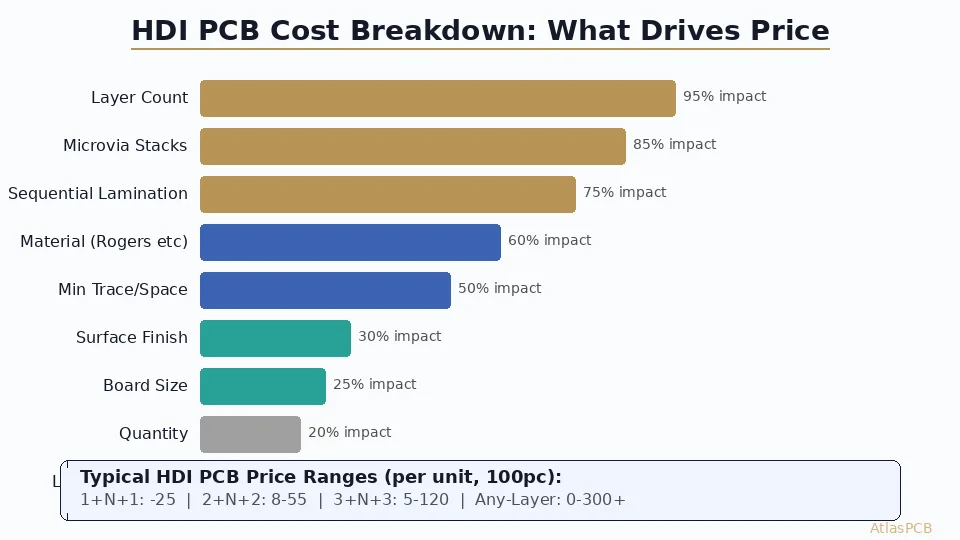
Cost Structure
| Cost Factor | Sequential | Build-Up |
|---|---|---|
| Base material | Standard prepreg + core | ABF film / RCC (3-5× material cost) |
| Drilling | Mechanical (fast, cheap) | Laser (slower, specialized) |
| Lamination cycles | 2-4 per board | 4-10+ per board |
| Registration | Standard | Precision (+20% cost) |
| Yield (mature) | 85-92% | 75-88% |
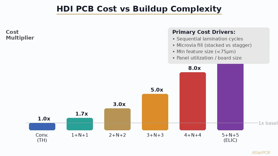
| Typical $/layer (relative) | 1.0× | 1.4-1.8× |
Manufacturing Lead Time
- Sequential lamination: 3-5 weeks for 16+ layer boards
- Standard build-up (1+N+1, 2+N+2): 4-6 weeks
- Any-layer HDI (3+N+3 and above): 5-8 weeks
Decision Framework: Which Process to Choose
Choose Sequential Lamination When:
- BGA pitch is ≥0.8 mm with manageable pin counts (<400)
- Design requires >2 oz copper on power planes
- Total layer count exceeds 20 (backplane-class)
- Budget constraints prohibit HDI premium
- Thermal cycling requirements exceed 2000 cycles
- Prototype turnaround is critical (faster in some regions)
Choose Build-Up HDI When:
- BGA/CSP pitch is ≤0.65 mm
- Package pin count exceeds available routing channels
- Board size is constrained (wearables, mobile, SiP modules)
- Signal integrity requires shorter via stubs
- High-speed serial links need controlled via impedance
- Weight reduction is critical (aerospace, portable devices)
Hybrid Approach: Sequential + Build-Up
Many modern designs combine both approaches:
- Core section: Sequential lamination for power distribution and ground planes
- Outer build-up layers: Microvia layers for high-density signal escape
This hybrid (designated in IPC notation as N+Core+N, e.g., 2+8+2) provides the best balance of density, reliability, and cost for designs like smartphones, automotive ADAS modules, and networking ASICs.
Material Selection Impact
Sequential Lamination Materials
- Standard FR-4 (Tg 170°C): Cost-effective for ≤10 Gbps designs
- High-Tg FR-4 (Tg 180-210°C): Required for lead-free assembly and high-reliability
- Low-Dk/Df laminates (Megtron 6, TU-872): For >10 Gbps signal integrity
- Polyimide: For extreme thermal environments (-65°C to +260°C)
Build-Up Materials
- ABF (Ajinomoto Build-up Film): Industry standard for any-layer HDI; Dk ~3.3 at 1 GHz
- RCC (Resin Coated Copper): Traditional build-up; lower cost than ABF
- Low-loss ABF variants: For 56+ Gbps applications (Df < 0.005 at 10 GHz)
- Photosensitive dielectric: Enables via formation without laser (limited to large vias)
Design for Manufacturability Tips
For Sequential Lamination
- Maintain drill-to-copper clearance ≥ 0.2 mm on all inner layers
- Avoid aspect ratios > 10:1 — request back-drill for thick boards
- Stagger buried vias between lamination cycles to avoid alignment stacking
- Include test coupons for buried via reliability verification
For Build-Up HDI
- Match via-in-pad to BGA pitch — don’t place microvias between pads
- Copper-fill all stacked vias — specify in fabrication notes
- Design for ±25 μm registration — account for layer shift in your clearances
- Use teardrop connections at microvia-to-trace junctions
- Keep build-up dielectric uniform — varying thickness degrades via reliability
Further Reading
- HDI Microvia Stacked vs Staggered: Reliability Comparison
- Any-Layer HDI PCB Design for Wearables and SiP
- 16-Layer PCB Stackup Design Guide
- PCB Stackup Symmetry and Balanced Lamination
Partner with AtlasPCB for Your HDI Manufacturing
Whether your design calls for sequential lamination with buried vias or advanced any-layer build-up with 50 μm microvias, AtlasPCB delivers production-quality HDI boards with IPC Class 3 reliability. Our engineering team provides free DFM analysis to optimize your stackup for manufacturing yield.
About AtlasPCB — We specialize in complex PCB manufacturing for HDI, RF, and high-reliability applications. Explore our HDI PCB manufacturing capabilities, multilayer PCB fabrication up to 30 layers, or get an full PCB manufacturing capabilities . Every order includes free engineering review. Get your quote.
Reviewed by AtlasPCB Engineering Team — IPC-certified manufacturing specialists with 15+ years of production experience in HDI, RF, and high-reliability PCB fabrication. Content based on factory floor data and real customer design reviews.
Frequently Asked Questions
What is the maximum layer count for build-up HDI vs sequential lamination?
How much does build-up HDI cost compared to sequential lamination?
When should I choose sequential lamination over build-up HDI?
- hdi pcb
- sequential lamination
- build-up
- microvia
- multilayer
- pcb manufacturing