· David Okafor · Engineering · 8 min read
JLCPCB vs Custom PCB Manufacturer in 2026
A practical comparison of when JLCPCB's automated prototyping model works — and when you need a dedicated custom PCB manufacturer with engineering support, advanced materials, and controlled impedance capabilities.
Quick Answer
Use JLCPCB for standard 2-4 layer FR-4 prototypes with relaxed specs. Switch to a custom PCB manufacturer when your design requires impedance control tighter than +/-10%, HDI microvias, Rogers/PTFE laminates, rigid-flex construction, or production volumes where yield consistency and engineering DFM review prevent costly respins.
Quick Decision: JLCPCB or Custom Manufacturer?
| Your Situation | Recommendation |
|---|---|
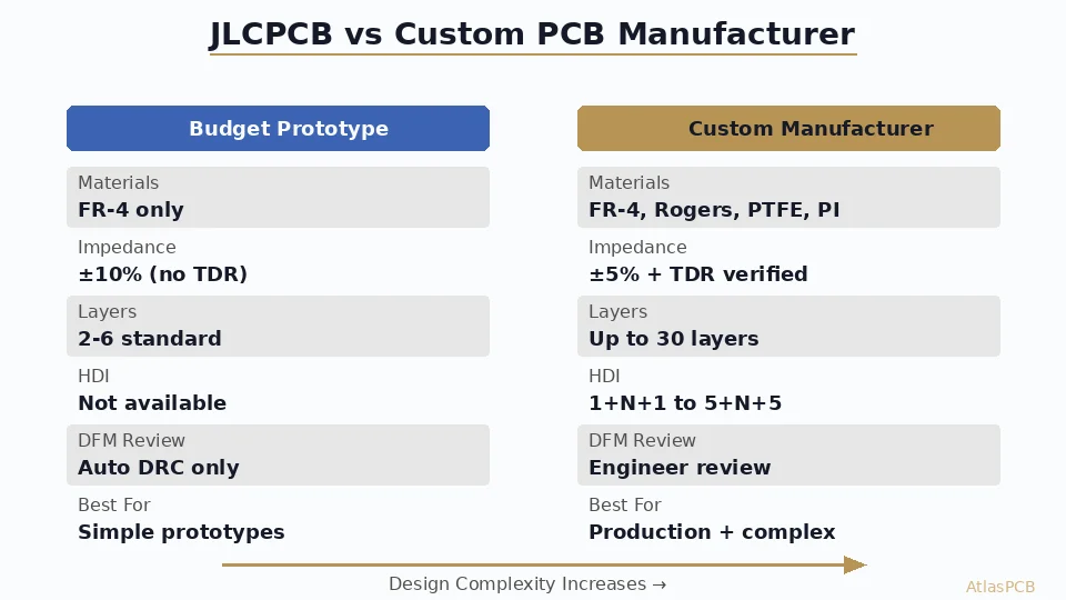
| 2-layer FR-4, 6/6mil, no impedance requirements | JLCPCB |
| 4-layer with basic impedance (+/-10% OK) | JLCPCB (with caveats) |
| 6+ layers, controlled impedance +/-5% | Custom manufacturer |
| HDI with microvias or via-in-pad | Custom manufacturer |
| Rogers, PTFE, or hybrid stackup | Custom manufacturer |
| Rigid-flex construction | Custom manufacturer |
| Production >500 pieces | Custom manufacturer (comparable pricing, better yield) |
| Medical/Aerospace compliance needed | Custom manufacturer (mandatory) |
If your design falls anywhere in the bottom half of this table, you are likely wasting money and time trying to force it through an automated prototyping service. The false economy of a cheap board that fails in testing costs far more than doing it right the first time.
The Core Difference: Automation vs Engineering
JLCPCB built a remarkably efficient business by automating everything that can be automated in PCB fabrication. Their order flow, panelization, and basic DRC checks run without human intervention, which is exactly how they deliver $2 boards with 24-hour turnaround. For simple designs within their standard capability window, this works beautifully.
The problem arises when engineers attempt to push complex designs through this same automated pipeline. There is no process engineer reviewing your stackup calculations. Nobody is checking whether your impedance targets are achievable with the available prepreg thicknesses. No one flags that your via-in-pad design needs specific plating parameters to avoid dimpling issues during reflow.
In our facility, we see approximately three boards per week that arrive as “rescue jobs” — designs that were fabricated at budget houses, failed testing, and now need urgent refabrication with proper engineering oversight. The most common failure mode is impedance being 15-20% off target because the stackup was never simulated against actual available material thicknesses. A custom manufacturer catches this during DFM review before a single panel enters production.
IMPEDANCE-CONTROLLED PCB MANUFACTURER
Need +/-5% Impedance Tolerance?
Our process engineers simulate your stackup against actual material inventory before production. Every panel ships with TDR-verified impedance test coupons.
Upload Your Gerber Files ›
Capability Comparison: Where the Lines Actually Fall
The marketing claims from budget PCB services often obscure the practical limitations. Here is what actually happens when you order beyond standard capabilities:
Materials and Stackup Control
JLCPCB stocks a limited selection of FR-4 laminates — primarily Shengyi S1000-2 and equivalent materials with Dk around 4.2-4.5 at 1 GHz. You cannot specify a particular prepreg style (1080, 2116, 7628) or request a specific core thickness. The system assigns materials based on availability and panel efficiency, which means your impedance will vary based on whichever laminate happens to be in stock that week.
A custom manufacturer maintains inventory of multiple prepreg styles and core thicknesses specifically because impedance-controlled designs require precise dielectric thickness to hit target values. When we quote a controlled-impedance board, the process engineer specifies exact materials — for example, 2x1080 prepreg at 0.076mm per ply for a 50-ohm stripline — and those materials are reserved for your order. The impedance simulation runs against these specific parameters, not generic averages.
Manufacturing Tolerances and Verification
| Parameter | JLCPCB Standard | Custom Manufacturer |
|---|---|---|
| Trace width tolerance | +/-1.5mil (typical) | +/-0.5mil (with LDI) |
| Impedance tolerance | +/-10% (no coupon) | +/-5% (TDR coupon per panel) |
| Dielectric thickness | +/-15% | +/-8% (controlled layup) |
| Registration accuracy | +/-3mil | +/-1.5mil (laser alignment) |
| Min via drill | 0.2mm mechanical | 0.075mm laser |
| Aspect ratio | 8:1 max | 16:1 (mechanical) |
These differences compound. A 15% variation in dielectric thickness plus 10% impedance tolerance means your 50-ohm trace could actually measure anywhere from 40 to 60 ohms — a range that causes visible eye diagram degradation on any signal above 5 Gbps.
The Hidden Cost Calculation Most Engineers Miss
The sticker price comparison — $5 at JLCPCB versus $150 at a custom shop — is misleading because it ignores the total cost of a design iteration. Based on panels we have run in the past quarter, here is what a typical “rescue job” actually costs an engineering team:
Scenario: 8-layer controlled-impedance board for USB4/Thunderbolt 4 application
Path A (JLCPCB first, then custom):
- JLCPCB prototype: $25 + $20 shipping = $45
- Testing reveals impedance failure: 2 engineering days lost = $1,600
- Respin at custom manufacturer: $180 + rush shipping $40 = $220
- Total: $1,865 + 2 weeks delay
Path B (Custom manufacturer from start):
- DFM review catches stackup issue, corrects before fabrication: 0 lost days
- Prototype: $180 + $30 shipping = $210
- Total: $210 + 5 days
The cost-conscious engineer who “saved” $135 on the prototype actually spent $1,655 more and lost two weeks. We see this pattern repeat consistently with high-speed digital designs, particularly DDR5 memory interfaces and PCIe Gen5 where impedance accuracy directly determines whether the link trains at full speed.
SKIP THE RESPIN CYCLE
DFM Review Before Production Starts
Our engineers review impedance stackups, check material availability, and flag DFM issues before your board enters the production queue. No surprises at testing.
View Our Capabilities ›When JLCPCB is the Right Choice
Credit where it is due — JLCPCB excels in specific scenarios and there is no reason to overspend when their service matches your needs:
Proof-of-concept boards where you are validating circuit functionality before committing to a final layout. A $5 board that proves your power supply topology works is perfectly rational before investing in a production-quality PCB.
Arduino shields and breakout boards with generous geometries, no controlled impedance, and purely digital signals below 100 MHz. The standard 6/6mil trace/space on FR-4 is more than adequate.
Student and maker projects where learning and iteration speed matter more than manufacturing precision. The ability to order five boards for the cost of lunch enables rapid experimentation.
Form factor validation — checking mechanical fit, connector placement, and enclosure compatibility before the final production order.
The key distinction is recognizing when your design has crossed the threshold from “prototype for learning” to “prototype for production validation.” If the board you are building needs to demonstrate that your product works at spec in the final configuration, that is not the time for a budget fab.
Production Volume: Where Custom Shops Compete on Price
A surprising reality that many engineers discover too late: at production volumes of 500-1000+ pieces, custom manufacturers frequently offer lower per-unit pricing than JLCPCB while delivering superior quality. The economics shift because:
First, custom shops optimize panelization for your specific board dimensions, achieving 85-92% panel utilization versus JLCPCB’s generic panelization that might waste 30-40% of panel area on odd-shaped boards. That material efficiency directly translates to per-unit cost.
Second, yield rates matter enormously at volume. A budget fab running at 85% yield on a complex board means you pay for 15% scrap built into the unit price. A custom manufacturer with process-specific recipes for your board achieves 95-98% yield on the same design, because the process engineer optimized drill parameters, etching chemistry, and press cycles for your specific stackup.
Third, there are no surcharges for “special” features. At JLCPCB, every deviation from standard (impedance control, blind vias, ENIG finish, via-in-pad) adds line-item costs. A custom manufacturer prices the complete board as a unit, and features like impedance control and via-in-pad are part of the standard production flow, not exceptions.
VOLUME PRODUCTION PRICING
Get a Production Quote — Often Lower Than You Expect
Upload your Gerber files for a production-volume quote. We optimize panelization and process parameters to minimize per-unit cost at 100-10,000+ piece quantities.
Get Production Quote ›Decision Flowchart: Which Supplier for Your Next Board
Start here: Does your design require ANY of the following?
- Impedance control tighter than +/-10%
- Layer count above 6
- Trace/space below 4/4mil
- Rogers, PTFE, or polyimide materials
- Blind/buried/stacked microvias
- Rigid-flex construction
- Via-in-pad with planarization
- IPC Class 3 or AS9100 compliance
- Production volume above 500 pieces
If YES to any of these: use a custom manufacturer. The cost difference is minimal compared to the risk of failure.
If NO to all: JLCPCB is a perfectly reasonable choice for your prototype.
This is not a quality judgment — it is a capability matching exercise. Use the right tool for the job.
ATLASPCB
Ready to Move Beyond Budget Prototyping?
From controlled-impedance high-speed digital to RF on Rogers — our process engineers ensure your board works the first time. Upload Gerbers for an engineering review and quote.
Get Engineering Review + Quote ›
Reviewed by AtlasPCB Engineering Team — 15+ years in advanced PCB fabrication for RF, HDI, and rigid-flex applications.
Related Reading:
About AtlasPCB — We specialize in complex PCB manufacturing for HDI, RF, and high-reliability applications. Explore our impedance-controlled PCB manufacturing . Every order includes free engineering review. Get your quote.
Reviewed by AtlasPCB Engineering Team — IPC-certified manufacturing specialists with 15+ years of production experience in HDI, RF, and high-reliability PCB fabrication. Content based on factory floor data and real customer design reviews.
Frequently Asked Questions
Is JLCPCB good enough for impedance-controlled PCBs?
When does the cost advantage of JLCPCB disappear?
Can JLCPCB fabricate Rogers or PTFE materials?
What are the risks of using JLCPCB for production runs?
How do custom PCB manufacturers handle DFM issues differently?
- JLCPCB
- custom PCB manufacturer
- impedance controlled PCB
- China PCB manufacturer
- PCB fabrication