· Marcus Lin · Engineering · 7 min read
PCB Design for LEO Satellites
Design PCBs that survive low-Earth orbit. Covers radiation-tolerant material selection, thermal cycling from -150°C to +120°C, outgassing per NASA ASTM E595, and vibration qualification for satellite and constellation hardware.
Quick Answer
PCB design for LEO satellites requires three critical adaptations: radiation-tolerant materials and shielding (total ionizing dose 10-50 krad over 5-year missions), extreme thermal cycling survival (-150°C to +120°C eclipse transitions every 90 minutes), and strict outgassing compliance (ASTM E595: TML <1.0%, CVCM <0.1%). The Starlink-driven constellation boom has created a new 'NewSpace' PCB tier—cost-sensitive but still requiring polyimide substrates, ENIG/ENEPIG finishes, and IPC-6012ES (Space Addendum) compliance.
The LEO Satellite PCB Challenge
Low-Earth orbit is one of the harshest operating environments for electronics. Every 90 minutes, a satellite circles the Earth, transitioning between direct solar exposure (+120°C) and eclipse darkness (-150°C). Add ionizing radiation, atomic oxygen erosion, vacuum-induced outgassing, and launch vibration — and you have a qualification environment that pushes PCB technology to its limits.
The explosion of LEO mega-constellations (Starlink, OneWeb, Amazon Kuiper) has created a new market segment: high-reliability PCBs at commercial production volumes. Traditional space-grade PCBs were hand-built in lots of 5-50 at costs exceeding $500/board. NewSpace constellations need thousands of boards monthly at $50-150/board while still surviving 5-7 year orbital lifetimes.
This guide covers the specific PCB design and material requirements for LEO applications, bridging the gap between heritage space programs and NewSpace production realities.
Thermal Environment and Material Selection
The Thermal Cycling Challenge
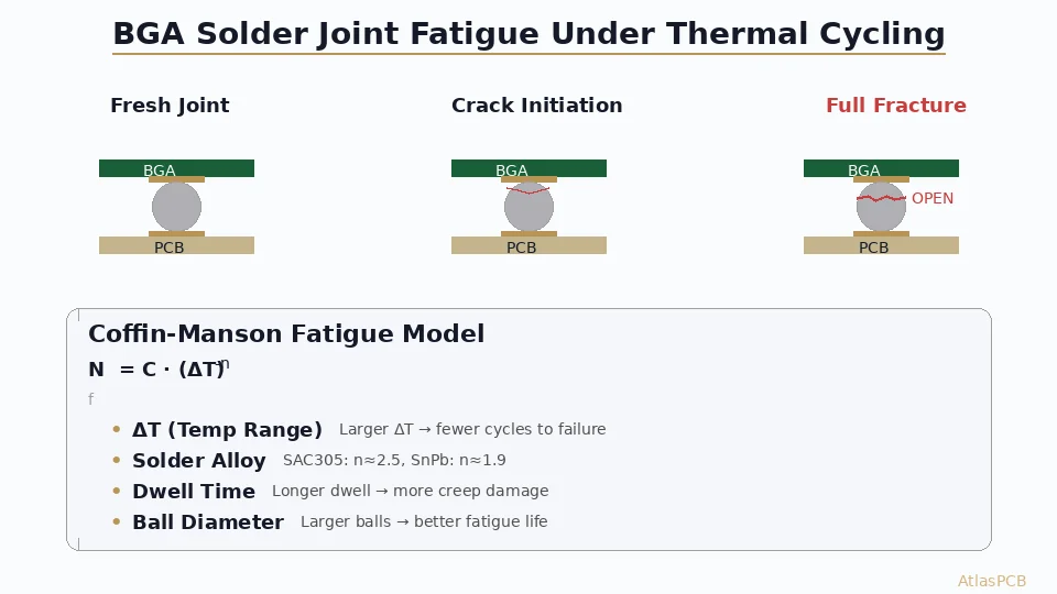
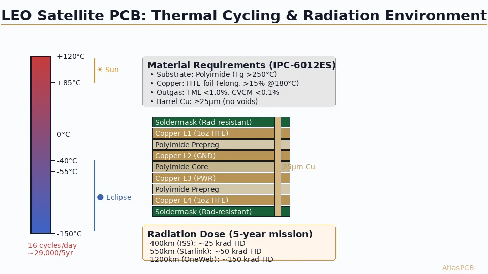
LEO orbit period: ~90 minutes → 16 thermal cycles per day → 5,840 cycles per year → 29,200 cycles over 5-year mission
Temperature range varies by satellite design:
- External panels (no thermal control): -150°C to +120°C
- Internal electronics (thermal management): -40°C to +85°C
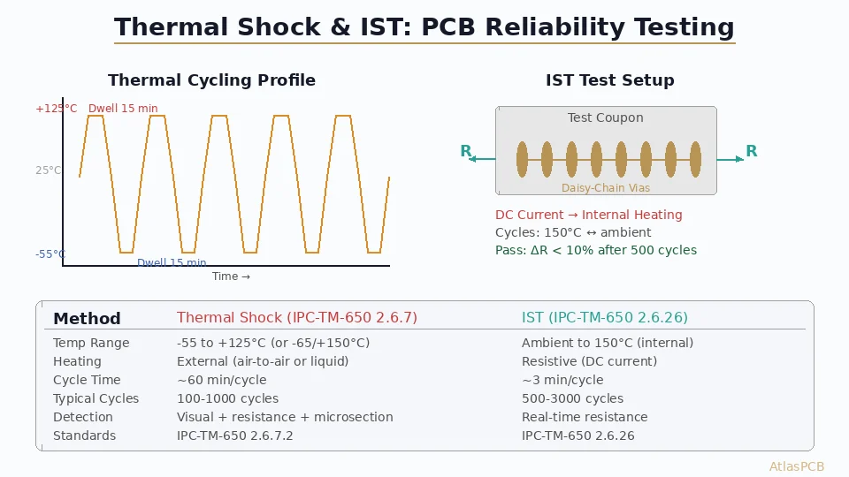
- Qualification testing: Typically -55°C to +125°C, 1000-2000 cycles per IPC-6012ES
Material Requirements
| Parameter | Standard FR-4 | High-Tg FR-4 | Polyimide (Space-Grade) |
|---|---|---|---|
| Tg | 130-170°C | 170-200°C | 250-280°C |
| Td (decomposition) | 300-330°C | 330-350°C | >400°C |
| TML (outgassing) | 1.0-2.0% | 0.5-1.0% | 0.1-0.3% |
| CTE (Z-axis) | 50-70 ppm/°C | 40-55 ppm/°C | 30-45 ppm/°C |
| Thermal cycling survival | <500 cycles | 500-1000 cycles | >5000 cycles |
| Radiation tolerance | Poor (50 krad) | Moderate (75 krad) | Excellent (200+ krad) |
| Relative cost | 1× | 1.5-2× | 3-5× |
Recommended materials for LEO:
- Mission-critical (>3 year life): Arlon 85N, Isola P96, Panasonic Megtron R-5775
- NewSpace cost-optimized (3-5 year): High-Tg polyimide: Isola 370HR + E595 screening
- Non-critical structures: Rogers/Arlon CLTE series for thermal stability
Copper Selection for Thermal Cycling
Copper foil ductility is critical for surviving repeated thermal strain:
- Standard ED copper: Elongation 5-12% → cracks after 2000-3000 aggressive cycles
- HTE (High-Temperature Elongation) copper: Elongation >15% at 180°C → standard for space
- RA (Rolled Annealed) copper: Elongation >20% → excellent fatigue resistance
For PTH (plated-through-hole) reliability, minimum barrel plating of 25µm (1 mil) copper is required per IPC-6012ES. Many programs specify 30-35µm for margin.
Radiation Environment
LEO Radiation Sources
- Trapped protons and electrons (Van Allen belts): Dominant at 500-2000km altitude
- Galactic cosmic rays (GCR): High-energy particles causing single-event effects
- Solar particle events (SPE): Sporadic high-flux proton storms
Total Ionizing Dose (TID) in LEO:
- 400km (ISS orbit): ~5 krad/year with 2mm Al shielding
- 550km (Starlink): ~8-12 krad/year
- 1200km (OneWeb): ~20-40 krad/year
Radiation Effects on PCB Materials
Epoxy degradation: Radiation breaks molecular cross-links → reduced adhesion, increased water absorption, lower peel strength. FR-4 loses 50% peel strength at 50 krad; polyimide retains 80% at 200 krad.
Soldermask embrittlement: Standard LPI soldermask becomes brittle and cracks after 30-50 krad. Space-qualified masks (e.g., Taiyo PSR-4000 AUS703) maintain flexibility to 100+ krad.
Conductive Anodic Filament (CAF): Radiation accelerates CAF growth along glass-resin interfaces. Prevention: Use tightly-woven glass styles (106, 1080) and maintain minimum 8 mil via-to-via clearance.
ENIG finish: No degradation from radiation. Immersion tin may form whiskers under combined radiation + thermal cycling stress — avoid for space applications.
Space & Aerospace PCB
IPC-6012ES Qualified Manufacturing
AtlasPCB manufactures PCBs compliant with IPC-6012ES Space Addendum requirements. Polyimide substrates, E595 outgassing screening, and full thermal cycling qualification data available.
View Space Capabilities →Outgassing: ASTM E595 Compliance
Why Outgassing Matters in Orbit
In vacuum, volatile compounds in PCB materials sublimate and migrate to cold surfaces. This molecular contamination:
- Degrades solar cells: 1% power loss per year from molecular film deposition
- Obscures optics: Camera lenses, star trackers, LIDAR receivers
- Alters thermal properties: Changes surface emissivity/absorptivity ratios
- Shorts electronics: Condensed films can bridge high-impedance circuits
E595 Test Method
Materials are heated to 125°C at <7×10⁻³ Pa for 24 hours:
- TML (Total Mass Loss): Weight loss of sample — must be <1.0%
- CVCM (Collected Volatile Condensable Material): Material deposited on a 25°C collector plate — must be <0.1%
- WVR (Water Vapor Regained): Weight regained after 24h at 50% RH — informational only
PCB Material Outgassing Data
| Material | TML (%) | CVCM (%) | Pass E595? |
|---|---|---|---|
| Standard FR-4 (Isola 370HR) | 0.80 | 0.02 | Marginal |
| Polyimide (Arlon 85N) | 0.25 | 0.01 | ✅ Yes |
| Rogers 4350B | 0.05 | 0.00 | ✅ Yes |
| LPI Soldermask (typical) | 0.40-0.90 | 0.03-0.08 | Varies |
| Conformal coat (Parylene C) | 0.10 | 0.01 | ✅ Yes |
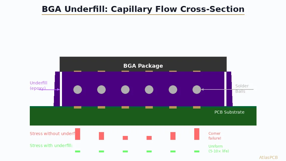
| Underfill (typical epoxy) | 1.2-2.5 | 0.05-0.20 | ❌ Often fails |
Critical: Every material layer must independently pass E595. A PCB can use space-grade substrate but fail due to non-compliant soldermask or marking ink.
Bake-Out Procedures
Pre-flight bake-out reduces initial outgassing:
- Standard bake: 125°C, 24 hours, vacuum or dry nitrogen
- Extended bake: 100°C, 72 hours for assemblies with moisture-sensitive materials
- Post-bake storage: Sealed nitrogen bags with desiccant until integration
Vibration and Mechanical Requirements
Launch Loads
Typical launch vibration environments for LEO deployment:
- Random vibration: 14.1 Grms (20-2000 Hz), 60 seconds per axis
- Sine vibration: 0.5-25g, 5-100 Hz sweep
- Shock: 1000-3000g SRS at >1000 Hz (pyrotechnic separation events)
- Quasi-static: 8-15g sustained acceleration
PCB Design for Vibration Survival
Board natural frequency: Must be >2× the highest sinusoidal excitation frequency. For typical satellite structures:
- Minimum first mode: >120 Hz for cards mounted on all 4 edges
- Critical: Use 2.0mm+ board thickness for cards >150mm span
Component attachment:
- Heavy components (>5g): Staked with epoxy dots at corners
- Tall components: Height-to-width ratio <2:1, or mechanically bracketed
- BGA: Underfill required for packages >15mm body size
Mounting:
- Edge-card guides with wedgelock clamps (not just friction fit)
- Thermal interface material doubles as vibration damper
- Avoid cantilevered mounting — support all edges where possible
IPC-6012ES (Space Addendum) Key Requirements
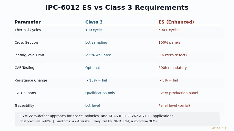
IPC-6012ES adds these requirements beyond standard IPC-6012E Class 3:
- Copper plating: Minimum 25µm barrel, no voids by microsection
- Innerlayer registration: ±50µm (vs. ±75µm for Class 3 terrestrial)
- Dielectric spacing: Minimum 75µm between conductors (vs. 50µm)
- Outgassing: All materials E595 compliant
- Thermal stress: 6× solder float at 288°C, no defects
- IST: 500 cycles minimum for qualification coupons
- Microsection: Per lot, all layer pairs sampled
- Ionic cleanliness: <1.56 µg NaCl/cm² equivalence
NewSpace vs. Heritage Space PCB Comparison
| Requirement | Heritage (GEO/Deep Space) | NewSpace (LEO Constellation) |
|---|---|---|
| Mission life | 15-20 years | 5-7 years |
| Radiation dose | 50-300 krad | 10-50 krad |
| Thermal cycles | 5,000-10,000 | 25,000-30,000 |
| Volume | 1-50 boards | 1,000-10,000/month |
| Substrate | Always polyimide | High-Tg or polyimide |
| Testing | 100% screening + qualification | Sample-based + qualification |
| Cost per board | $500-5,000 | $50-200 |
| Lead time | 12-20 weeks | 4-8 weeks |
| Standard | MIL-PRF-31032 + ESCC | IPC-6012ES + workmanship |
The NewSpace paradigm accepts higher risk at lower cost — using commercial manufacturing processes with space-qualified materials rather than fully bespoke space manufacturing.
Design Checklist for LEO PCBs
Material Selection
- Substrate Tg >200°C (polyimide or equivalent)
- All materials E595 screened (TML <1.0%, CVCM <0.1%)
- Copper: HTE or RA foil for thermal cycling fatigue resistance
- Soldermask: Space-qualified (radiation-resistant to mission TID)
- Surface finish: ENIG or ENEPIG (no immersion tin)
Stackup Design
- Minimum copper thickness: 25µm barrel after plating
- Board thickness adequate for first-mode frequency requirement
- Symmetric stackup for warpage control during thermal cycling
- Via aspect ratio ≤10:1 for reliable plating
Layout
- Minimum spacing per IPC-6012ES (75µm conductor-to-conductor)
- Via-to-via spacing ≥8 mil (CAF prevention)
- Heavy component staking provisions (epoxy dot pads)
- Strain-relief for flex-rigid transitions
- Thermal relief pads for all power/ground vias
Qualification
- Thermal cycling: -55°C to +125°C, 1000 cycles minimum
- Vibration: Random + sine per launch vehicle environment
- Outgassing: Board-level E595 verification (not just material datasheets)
- IST: 500 cycles, <5% resistance change
- Microsection: All layer pairs, 6 locations per coupon panel
Market Trends: LEO Constellation PCB Demand
The Starlink constellation alone contains approximately 7,000+ active satellites as of 2026, each containing multiple PCB assemblies. Combined with OneWeb (~650 satellites), Amazon Kuiper (planned 3,236), and dozens of smaller constellations, the LEO PCB market has grown from a niche aerospace segment to a significant volume opportunity.
Key demand drivers:
- Per-satellite PCB content: 8-15 board assemblies (power, comms, processing, antenna)
- Replacement cycle: Satellites deorbit after 5-7 years → continuous replenishment
- Ground infrastructure: Each constellation requires 50-200 ground stations with high-frequency PCB assemblies
This has created a new fabricator capability tier — companies that can deliver IPC-6012ES quality at commercial volumes and lead times.
Further Reading
- RF Microwave PCB Design Guide
- PCB Thermal Management Strategies
- Controlled Impedance PCB Stackup Design Rules
- What Is Rogers PCB Material?
Designing PCBs for orbit? Contact our aerospace team for material recommendations, IPC-6012ES compliance guidance, and production quotation. We support both heritage space programs and NewSpace constellation volumes.
About AtlasPCB — We specialize in complex PCB manufacturing for HDI, RF, and high-reliability applications. Explore our aluminum and metal-core PCB services . Every order includes free engineering review. Get your quote.
Reviewed by AtlasPCB Engineering Team — IPC-certified manufacturing specialists with 15+ years of production experience in HDI, RF, and high-reliability PCB fabrication. Content based on factory floor data and real customer design reviews.
Frequently Asked Questions
Can FR-4 be used in LEO satellite PCBs?
How does radiation affect PCB materials in LEO?
What is the outgassing requirement for satellite PCBs and why does it matter?
- satellite-pcb
- leo
- radiation-hardening
- space-electronics
- aerospace
- thermal-cycling