· AtlasPCB Engineering · Engineering · 12 min read
PCB DFM Check: 12 Critical Errors That Delay Your Board and How to Catch Them Before Submission
A production engineer's checklist of the most common DFM violations we catch during Gerber review — from annular ring violations and acid traps to impedance stackup mismatches. Each error includes the IPC standard reference, why it causes rejection, and how to fix it in your CAD tool before submitting files.
Quick Answer
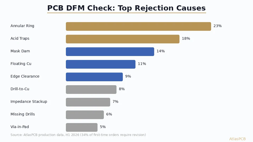
The 12 most frequent DFM errors that delay PCB fabrication are: insufficient annular ring (IPC-6012 Class 2 minimum 5mil), acid traps under 90 degrees, missing solder mask dams between SMD pads (minimum 3mil), unconnected copper pours creating floating copper, trace-to-edge clearance below 10mil, drill-to-copper violations, incorrect layer stackup for impedance targets, missing drill files or aperture definitions, via-in-pad without filled/capped specification, solder paste stencil errors, panelization conflicts, and silkscreen overlap on pads.
The Problem: 34% of First-Time PCB Orders Have DFM Errors
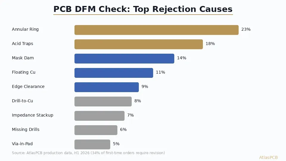
Based on our production data from the first half of 2026, approximately one-third of new customer orders require at least one design revision before manufacturing can begin. Each revision cycle adds 1-3 days to your delivery timeline. For engineers on tight prototype schedules, a preventable DFM error can mean the difference between validating hardware this sprint or pushing to the next.
The frustrating part is that most DFM errors are entirely predictable. They cluster into the same 12 categories across thousands of designs. An engineer who spends 30 minutes running through this checklist before submitting Gerber files will avoid the most common delays. This is not about perfect design — it is about catching the issues that stop a board from entering production.
The 12 Critical DFM Errors (Ranked by Frequency)
1. Annular Ring Violations (23% of rejections)
The annular ring is the copper pad remaining around a drilled hole after manufacturing tolerances are applied. IPC-6012 Class 2 requires a minimum 5mil (0.127mm) annular ring. Class 3 (aerospace, medical) requires 5mil minimum with no breakout permitted.
The mistake happens when designers use via definitions from older libraries or competitor templates without verifying pad-to-drill relationships. A common failure: using a 0.3mm drill with a 0.5mm pad. On paper, that is 0.1mm (4mil) annular ring per side — already below Class 2 minimum before accounting for drill registration tolerance (typically +/-2mil) and etch compensation.
Fix: Minimum pad diameter = drill size + 10mil (0.25mm) for Class 2. For 0.3mm drills, use 0.55mm pads minimum. In Altium, check Design Rules > Manufacturing > Minimum Annular Ring. In KiCad, set the annular ring DRC to 0.125mm minimum.
2. Acid Traps and Acute Angles (18% of rejections)
Acute-angle trace junctions below 90 degrees create etching problems. The etchant becomes trapped in the sharp interior angle, over-etching the copper and potentially creating opens or weakened conductors. This is particularly problematic at fine-pitch routing (3/3mil or 4/4mil trace/space) where any over-etch is proportionally significant.
Our AOI (Automated Optical Inspection) system flags these during post-etch verification, but the board has already been etched by then. If the over-etch creates an electrical open, the panel is scrapped. We see this most frequently on BGA breakout routing where designers manually route traces at non-orthogonal angles to reach inner vias.
Fix: Ensure all trace junctions are 90 degrees or greater. Use 45-degree routing rather than arbitrary angles. In your CAD tool, run an acute angle check with a threshold of 90 degrees. Most modern EDA tools have this as a standard DRC rule but it is often disabled by default.
3. Solder Mask Dam Violations (14% of rejections)
The solder mask dam is the strip of mask material between adjacent SMD pad openings. When this dam falls below the minimum width (typically 3mil/75um for LPI solder mask), the mask cannot reliably form between pads. The result: solder bridges during assembly, particularly on fine-pitch QFP and BGA packages.
For HDI PCBs with 0.4mm-pitch BGAs, designers often expand mask openings for better soldering without considering the resulting dam width. A 0.4mm pitch BGA with 0.25mm pad openings leaves only 0.15mm (6mil) mask dam — adequate. But expanding openings to 0.3mm (common for better wetting) reduces the dam to 0.1mm (4mil) — still above minimum but risky for yield.
Fix: Check mask-to-mask clearance on all fine-pitch components. Minimum 3mil dam for standard LPI mask, 2mil for advanced LDI (laser direct imaging) processes. If your manufacturer uses LDI (as we do for fine-pitch boards), you can achieve 2mil dams reliably, but always confirm before assuming.
DFM REVIEW INCLUDED
Catch These Errors Before Production
Every AtlasPCB order includes engineering DFM review. We flag issues with marked-up screenshots and suggest fixes before manufacturing starts.
Submit Files for Review ›
4. Floating Copper and Unconnected Pours (11% of rejections)
Copper pour regions that are not connected to any net create two problems. First, they act as antennas that can couple noise into adjacent signal traces. Second, during the etching process, small isolated copper features may detach from the substrate and contaminate the etching line, potentially causing defects on other panels in the same batch.
Most CAD tools generate copper pours with a “remove dead copper” option, but this is often disabled during initial pour generation. The result: small copper islands remain in the design, particularly in areas between closely-spaced vias or near board edges where the pour algorithm cannot create a valid connection.
Fix: After generating all copper pours, run a DRC specifically checking for unconnected copper. In Altium, use Design > Rules > Electrical > Un-Connected Pad. In KiCad, run the ERC and look for unconnected copper zones. Remove islands smaller than 0.5mm square — they serve no electrical purpose and create manufacturing risk.
5. Trace-to-Edge Clearance Violations (9% of rejections)
Board edge routing (V-scoring or tab-routing) has mechanical tolerances. A V-score groove typically has +/-4mil position accuracy, while tab routing (profile milling) has +/-4-8mil depending on cutter diameter and fixturing method. Copper traces running too close to the board edge risk being exposed or nicked during depaneling.
IPC-6012 requires minimum 10mil (0.25mm) copper-to-edge clearance for external layers and 15mil for internal layers (due to edge sealing requirements). Many designers place ground pours extending to the board edge without applying proper pullback rules.
Fix: Apply a board-edge clearance rule of 10mil minimum for external copper and 15mil for internal layers. For RF boards with edge-mounted connectors requiring ground continuity to the edge, specify “copper to board edge” as a controlled feature in your fabrication notes so the manufacturer knows it is intentional.
6. Drill-to-Copper Clearance Errors (8% of rejections)
Non-plated holes (mounting holes, tooling holes) must maintain adequate clearance to copper on all layers. A NPTH with insufficient clearance to an internal power plane will drill through live copper, creating a short circuit or a reliability concern (copper burr touching an unintended net during vibration or thermal cycling).
The minimum drill-to-copper clearance for NPTH is 10mil beyond the drilled hole diameter on all layers. This accounts for drill wander, copper registration tolerance, and a safety margin for burr formation.
Fix: Check all NPTH hole definitions for copper clearance on every layer including internal planes. In your CAD tool, ensure NPTH holes have anti-pad definitions on all copper layers, not just the external layers. This is a common oversight when adding mounting holes late in the design process.
7. Impedance Stackup Infeasibility (7% of rejections)
Engineers specify target impedance values (typically 50 ohm single-ended, 100 ohm differential) without verifying that the stackup structure can achieve those values with available prepreg thicknesses. A common scenario: requesting 50 ohm microstrip with a 3.5mil trace on a 4mil dielectric — the required dielectric height to achieve 50 ohms with that trace width is approximately 5.2mil, which does not match any standard prepreg thickness.
In our facility, we solve approximately 60% of these cases by adjusting trace width within the customer’s routing constraints. The remaining cases require a dielectric height change, which may mean substituting a different prepreg or adjusting the stackup layer arrangement.
Fix: Before finalizing your design, use a 2D field solver (Polar Si9000, Saturn PCB Toolkit, or your manufacturer’s stackup tool) to verify that your impedance targets are achievable with your specified stackup. If you are unsure about available prepreg thicknesses, request a stackup proposal from your manufacturer before routing — this takes 1-2 days and prevents weeks of rework.
IMPEDANCE STACKUP DESIGN
Get a Verified Stackup Before You Route
Submit your layer count and impedance requirements. We provide a manufacturable stackup proposal with exact prepreg specs within 24 hours.
8. Missing or Incorrect Drill Files (6% of rejections)
This seems basic, but incomplete drill data causes significant delays because the manufacturer cannot proceed without clarification. Common problems: missing NPTH drill file (designer exports only the plated drill file), mixed plated and non-plated holes in a single drill file without proper tool differentiation, imperial/metric unit mismatch between Gerber and drill files, and missing back-drill specifications for controlled-depth drilling.
For HDI boards with laser vias, each via span requires its own drill file. A 2+N+2 HDI board needs: one through-drill file, two microvia files (L1-L2 and L(N-1)-LN at minimum), and potentially blind via files for inner layer connections. Missing any one of these files means the CAM engineer cannot generate the production tooling.
Fix: Create a drill file checklist matching your stackup: one file per drill span, clearly named. Include a fabrication drawing showing the drill span diagram (which layers each drill type connects). Use ODB++ or IPC-2581 intelligent formats that embed this information structurally rather than relying on file naming conventions.
9. Via-in-Pad Without Proper Specification (5% of rejections)
Modern BGA packages with 0.8mm pitch or finer require via-in-pad construction — vias placed directly in the component pad rather than fanned out to adjacent pads. The manufacturing options include: filled and capped (copper-filled, then plated over), filled with epoxy (non-conductive fill), or open via-in-pad (acceptable only for wave solder or selective solder applications).
The DFM error occurs when designers use via-in-pad without specifying the fill type in their fabrication notes. An unfilled via-in-pad will wick solder during reflow, creating voids under BGA balls and potentially causing open joints. If the manufacturer assumes standard (unfilled) vias because no fill specification is given, the board will fail at assembly.
Fix: Always specify via-in-pad treatment in your fabrication notes: “Via-in-pad: copper-filled and capped per IPC-4761 Type VII” is the standard call-out for BGA applications. Add this to your fab drawing clearly, not buried in general notes.
10. Solder Paste Stencil Conflicts (4% of rejections)
While stencil design is technically an assembly concern rather than fabrication, we flag paste layer issues during DFM because correcting them after boards are built wastes the entire assembly setup. Common problems: paste openings that extend beyond the mask opening (creating solder balls), paste openings on thermal relief pads that are too large (causing tombstoning on small passives), and paste layer data that uses the wrong aperture format.
Fix: Verify that paste openings are 1:1 with or slightly reduced from mask openings for all components. For 0201 and 01005 passives, use 80-90% paste-to-pad area ratio. For large thermal pads, use a windowed/segmented paste pattern (typically 50-60% coverage) to prevent voiding.
11. Panelization Conflicts (3% of rejections)
When boards are submitted without panelization instructions, the manufacturer creates a panel layout to maximize material utilization. Conflicts arise when board geometry, connector placements, or edge features prevent efficient panelization. Boards with overhanging connectors, non-rectangular outlines, or internal cutouts require specific panelization approaches that may add cost.
Fix: If your board has unusual geometry, include a panelization suggestion in your fabrication package. Specify your preferred breakaway method (V-score, tab-route, or perforated tab) and identify any areas that cannot have panel tabs (connector edges, antenna sections, flex portions).
12. Silkscreen on Pads (2% of rejections)
Silkscreen printing on exposed copper pads or SMD pads interferes with solderability. The silkscreen ink acts as a solder resist, preventing wetting and causing assembly defects. This typically happens when reference designators are auto-placed by the CAD tool without respecting pad clearances, or when component outlines overlap adjacent pads.
Fix: Apply silkscreen-to-pad clearance rules: minimum 4mil clearance between silkscreen and any pad or mask opening. In Altium, set Design Rules > Manufacturing > Silkscreen Over Component Pads to “Error.” Run a final DRC check after completing silkscreen placement and before generating outputs.
Pre-Submission DFM Checklist (Save This)
Before exporting your final Gerber package, verify:
- Annular ring: minimum 5mil on all vias and PTH pads
- No acute angle trace junctions (all junctions 90 degrees or greater)
- Solder mask dams: minimum 3mil between all adjacent pad openings
- No floating copper or unconnected pour islands
- Board edge clearance: 10mil external, 15mil internal
- NPTH holes have anti-pads on ALL copper layers
- Impedance verified with field solver against actual prepreg thicknesses
- Drill files complete: one per span, PTH/NPTH separated
- Via-in-pad specification clearly stated in fab notes
- Paste layer verified against mask layer openings
- Panel tab locations identified (if irregular board shape)
- Silkscreen cleared from all pads by minimum 4mil
This checklist takes 20-30 minutes to run through but saves 1-3 days of review-revision cycles. Engineers who submit clean files consistently receive boards 2-3 days faster than those who rely entirely on manufacturer DFM review to catch design issues.
ATLASPCB
Submit Your Files — We Handle the DFM
Every order gets a full engineering DFM review. We catch problems before they become expensive delays. Upload Gerbers, get a quote and DFM report within 24 hours.
Upload Gerber Files ›
Reviewed by AtlasPCB Engineering Team — 15+ years in advanced PCB fabrication for RF, HDI, and rigid-flex applications.
Related Reading:
About AtlasPCB — We specialize in complex PCB manufacturing for HDI, RF, and high-reliability applications. Explore our HDI PCB manufacturing capabilities, impedance-controlled PCB manufacturing, or get an free engineering DFM review . Every order includes free engineering review. Get your quote.
Reviewed by AtlasPCB Engineering Team — IPC-certified manufacturing specialists with 15+ years of production experience in HDI, RF, and high-reliability PCB fabrication. Content based on factory floor data and real customer design reviews.
Frequently Asked Questions
What is the most common DFM error that delays PCB fabrication?
How long does a DFM check take before PCB manufacturing starts?
Should I run DFM checks in my CAD tool before sending to the manufacturer?
What file formats does a manufacturer need for a complete DFM check?
Do I need to pay for DFM review before getting a PCB quote?
- PCB DFM check
- impedance controlled PCB manufacturer
- PCB stackup design guide
- HDI PCB manufacturer
- design for manufacturability