· AtlasPCB Engineering · Engineering · 10 min read
PCB Stackup Design Guide 2026: Layer Assignment, Impedance Planning, and Material Selection for 4 to 16 Layers
A step-by-step guide to designing PCB stackups from scratch. Covers layer assignment strategy, impedance-driven dielectric selection, reference plane placement, and manufacturer coordination to avoid costly stackup respins.
Quick Answer
Start stackup design by identifying your impedance targets and signal speed requirements, then work backward to determine layer count, dielectric thicknesses, and material grade. Every signal layer must be adjacent to a continuous reference plane. Coordinate with your PCB manufacturer early — they have actual prepreg thickness data and Dk values that differ from catalog specs, and catching stackup issues before layout saves 2-4 weeks versus discovering them at DFM review.
The Fundamental Principle: Every Signal Needs a Reference
Before discussing specific layer counts or material choices, internalize the single most important stackup rule: every signal trace carrying frequencies above 50 MHz must be routed adjacent to a continuous reference plane. Violating this principle — routing a high-speed signal between two signal layers, or over a plane split — creates EMI, crosstalk, and impedance discontinuities that no amount of termination or shielding can fully remediate.
This rule drives everything else in stackup design. It determines minimum layer count (you need enough planes to provide references for all your signal layers), plane placement (adjacent to every signal layer, no exceptions), and sometimes layer assignment (moving signals to different layers to maintain reference continuity).
Step 1: Inventory Your Requirements
Before opening your stackup tool, list the constraints that will drive your design:
Signal types and speeds: Categorize your signals into speed tiers. Below 100 MHz requires basic reference but no controlled impedance. 100 MHz to 5 GHz needs controlled impedance with standard tolerance. Above 5 GHz demands tight tolerance impedance control and potentially specialty materials.
Impedance targets: Identify all controlled impedance structures needed. Common targets: 50 ohm single-ended (microstrip and stripline), 85-100 ohm differential (USB, Ethernet, PCIe). List each target with the routing layer and reference configuration.
Power domains: Count distinct voltage rails requiring dedicated planes or large pours. Each plane consumes a layer. High-current domains (>5A) typically need dedicated planes; low-current domains can share split planes (but not under high-speed signals).
Routing density: Estimate the total routing demand from your component placement. BGA breakout fanout, bus routing width, and escape routing all consume channels. If routing demand exceeds available channels on signal layers adjacent to planes, you need more layers.
Thermal requirements: Power dissipation affects material selection (high-Tg requirement), copper weight (heavy copper for thermal spreading), and potentially embedded thermal vias or coin insertion.
STACKUP ENGINEERING
Get a Manufacturer-Validated Stackup Before You Start Layout
Send us your impedance targets and layer count estimate. We propose a stackup using our actual available materials and characterized Dk values — not catalog assumptions.
Request Stackup Proposal ›
Step 2: Choose Your Layer Count and Assignment Strategy
4-Layer Stackup (The Universal Starting Point)
The standard 4-layer stackup is the most cost-effective controlled impedance structure:
Layer 1: Signal (top) — microstrip, referenced to L2
Layer 2: Ground plane — primary reference, unbroken
Layer 3: Power plane — secondary reference
Layer 4: Signal (bottom) — microstrip, referenced to L3
This works for designs with moderate routing density and signal speeds up to 3-5 Gbps. The critical constraint: Layer 2 must remain an unbroken ground plane. Any splits in L2 directly degrade L1 signal integrity. Route power distribution on L3 and accept that L4 signals reference a potentially split power plane — or keep L3 unbroken and distribute power on L1/L4 using pours.
For a standard 1.6mm board thickness, the core between L2-L3 is typically 1.0-1.2mm, with prepreg layers of 0.1-0.2mm between signal and plane layers. This geometry naturally produces approximately 50 ohm for a 5-6 mil trace on standard FR-4 (Dk ~4.2 at the operating frequency).
6-Layer Stackup (First Step Up)
When 4 layers cannot accommodate your routing or you need a dedicated signal layer with stripline impedance:
Layer 1: Signal — microstrip, ref L2
Layer 2: Ground — primary reference
Layer 3: Signal — stripline, ref L2 and L4
Layer 4: Power — reference for L3 and L5
Layer 5: Signal — stripline, ref L4 and L6
Layer 6: Ground — bottom reference
This is the minimum layer count that provides stripline routing (signals sandwiched between two planes). Stripline offers better EMI containment and crosstalk isolation than microstrip, making it preferred for high-speed signals above 5 Gbps.
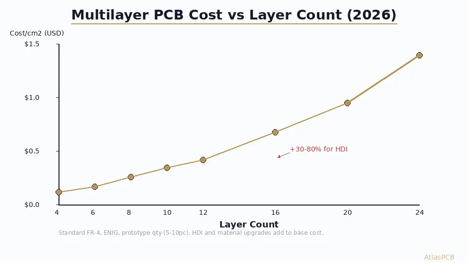
The cost step from 4 to 6 layers is significant (40-60% increase) because it requires an additional lamination cycle. However, if your design needs controlled impedance on internal layers, 6 layers is the minimum viable option — you cannot achieve stripline on a 4-layer board.
8-Layer Stackup (High-Speed Digital Standard)
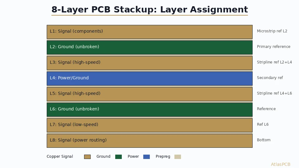
The 8-layer stackup is the workhorse for high-speed digital designs with DDR4/5, PCIe Gen4/5, and multi-gigabit Ethernet:
Layer 1: Signal (components, short high-speed traces) — ref L2
Layer 2: Ground — primary reference (unbroken)
Layer 3: Signal (high-speed routing) — stripline, ref L2+L4
Layer 4: Power/Ground — reference for L3 and L5
Layer 5: Signal (high-speed routing) — stripline, ref L4+L6
Layer 6: Ground — reference (unbroken)
Layer 7: Signal (low-speed, power routing) — ref L6
Layer 8: Signal (components, power) — ref L6 via prepreg
Note: L7 and L8 share reference from L6 — keep only low-speed signals here. All high-speed routing belongs on L3/L5 where stripline geometry provides maximum shielding.
For PCIe Gen5 designs, this 8-layer approach works when combined with ±5% impedance tolerance and low-loss prepreg (Dk ~3.8-4.0, Df < 0.01 at 10 GHz) on the critical signal layers.
MULTILAYER EXPERTISE
4 to 30 Layer Stackups — Impedance Controlled
FR-4, high-Tg, low-loss (Megtron, TU-872), and Rogers materials. We propose optimized stackups matching your impedance targets to our actual material inventory.
Upload Design ›Step 3: Material Selection — Matching Material Grade to Signal Speed
Material selection is driven by signal frequency content, not marketing claims. The critical parameters are:
Dk (Dielectric Constant): Affects trace width for target impedance. Higher Dk = narrower traces for same impedance. Standard FR-4 Dk ranges from 4.0-4.5 depending on frequency and resin content. Low-loss materials (Megtron 4/6, TU-872, Panasonic R-5775K) offer Dk around 3.4-3.8.
Df (Dissipation Factor / Loss Tangent): Determines signal attenuation. Standard FR-4 Df is 0.018-0.025 at 1 GHz. Mid-loss materials (Megtron 4, TU-862) achieve 0.008-0.012. Ultra-low-loss (Megtron 6, TU-872) reaches 0.003-0.005.
Material Selection by Application Speed
| Data Rate | Acceptable Df (10 GHz) | Material Grade | Examples |
|---|---|---|---|
| < 5 Gbps | 0.020-0.025 | Standard FR-4 | TU-662, IT-180A |
| 5-16 Gbps | 0.010-0.015 | Mid-loss | Megtron 4, TU-862, Panasonic R-5775G |
| 16-56 Gbps | 0.004-0.008 | Low-loss | Megtron 6, TU-872, Panasonic R-5775K |
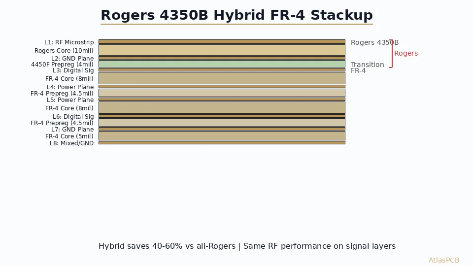
| > 56 Gbps | < 0.004 | Ultra-low-loss | Megtron 7, Rogers 4350B |
In our production, we stock standard FR-4 (TU-662/IT-180A), mid-loss (Megtron 4 equivalent), and low-loss (Megtron 6 equivalent) materials in common thicknesses. Specifying an exotic material not in standard stock adds 1-2 weeks lead time and potentially higher minimum order quantities.
Step 4: Impedance Calculation and Manufacturer Coordination
Why Catalog Dk Values Are Not Accurate Enough
Here is where most engineers make their first stackup mistake: they design using laminate manufacturer catalog Dk values, complete their layout assuming those values produce the target impedance, and then discover during manufacturing DFM review that the actual pressed Dk differs.
The reason: catalog Dk is measured on a pure laminate sample under controlled lab conditions. In a real pressed PCB, the effective Dk changes due to resin flow during lamination (which varies with press pressure, temperature profile, and the copper pattern density on adjacent layers). A prepreg specified at Dk 4.2 might press to an effective Dk of 3.9-4.1 depending on copper balance.
A competent PCB manufacturer maintains a database of actual pressed Dk values for their standard material combinations — characterized through production impedance coupon data, not theoretical calculations. This is why early coordination with your manufacturer matters: they can provide realistic Dk values that make your impedance calculation accurate the first time.
In our stackup review process, we correlate TDR data from thousands of production panels to build effective Dk models for each material/thickness combination in our inventory. When an engineer sends impedance targets, we propose layer thicknesses using these characterized values rather than catalog specifications.
The Coordination Workflow That Prevents Respins
- Before layout: Send impedance targets + estimated layer count to manufacturer
- Manufacturer proposes: Stackup with specific prepreg/core thicknesses from their inventory, using characterized Dk values
- Designer validates: Import proposed stackup into EDA tool, verify trace widths are manufacturable (above minimum etch capability)
- Iterate if needed: If trace widths are too narrow, adjust dielectric thickness or consider different Dk material
- Lock stackup: Document agreed stackup in fabrication drawing before starting detailed routing
This process adds 3-5 days at the start of your project but eliminates the common scenario of completing layout, sending to fab, receiving DFM feedback that the stackup needs modification, and then re-routing — a 2-4 week setback.
PRE-LAYOUT STACKUP REVIEW
Lock Your Stackup Before Routing — Save Weeks
Our engineers validate stackup feasibility against actual available materials and return a buildable proposal within 24-48 hours. Start routing with confidence.
Submit Stackup for Review ›Common Stackup Design Mistakes (What We See in DFM Review)
Based on reviewing hundreds of stackup designs monthly, these are the most frequent issues our process engineers catch:
Asymmetric stackups: Unbalanced copper distribution between top and bottom halves causes warpage during lamination. The board curves toward the side with more copper because differential CTE stress is unequal. Solution: mirror the copper weight distribution about the board center. If you have 2oz copper on L1, put 2oz on the bottom layer too.
Signal layers without adjacent reference: Engineers sometimes place two signal layers adjacent to each other (no plane between them) to save layer count. This creates severe crosstalk between the layers — signals couple broadside across the thin prepreg, with no shielding. Every signal layer must have at least one adjacent plane.
Incorrect via antipads disrupting reference planes: A field of via antipads can create effective “plane holes” that disrupt the return current path for signals routing nearby. When drilling vias through a reference plane, ensure the remaining copper provides a continuous path for return currents of all signals referencing that plane.
Mixing plane split boundaries with signal routing: A signal crossing a plane split (even in an adjacent reference layer) experiences a large impedance discontinuity and creates EMI as the return current must find an alternate path. If you must split a power plane, route signals only over areas where the plane is continuous, or stitch across splits with decoupling capacitors.
Summary: Stackup Design Checklist
Before sending your design for fabrication, verify:
- Every high-speed signal layer has an adjacent continuous reference plane
- Stackup is symmetric about the center (copper balance)
- Impedance targets are achievable with manufacturer’s available dielectric thicknesses
- Material grade matches your highest signal speed requirement
- No signal routing crosses plane splits in reference layers
- Power distribution does not compromise signal integrity reference planes
- Via fields do not create return current discontinuities
- Manufacturer has confirmed material availability and proposed specific thicknesses
ATLASPCB
Ready to Finalize Your Stackup? Start with Engineering Review.
Upload your requirements or preliminary stackup. Our process engineers validate against actual material inventory and return an optimized, buildable proposal. 4 to 30 layers, standard to low-loss materials.
Get Stackup Review ›
Reviewed by AtlasPCB Engineering Team — 15+ years in advanced PCB fabrication for RF, HDI, and rigid-flex applications.
Related Reading:
About AtlasPCB — We specialize in complex PCB manufacturing for HDI, RF, and high-reliability applications. Explore our impedance-controlled PCB manufacturing . Every order includes free engineering review. Get your quote.
Reviewed by AtlasPCB Engineering Team — IPC-certified manufacturing specialists with 15+ years of production experience in HDI, RF, and high-reliability PCB fabrication. Content based on factory floor data and real customer design reviews.
Frequently Asked Questions
How do I decide how many layers my PCB needs?
Should signal layers reference ground or power planes?
When should I choose high-Tg material versus standard FR-4?
How early should I involve my PCB manufacturer in stackup design?
What is the cost impact of adding 2 more layers?
- PCB stackup design guide
- impedance controlled PCB
- PCB manufacturer
- multilayer PCB
- high-speed PCB design