· AtlasPCB Engineering · Engineering · 9 min read
Impedance Controlled PCB: Standard ±10% vs Tight ±5% Tolerance — Cost, Applications, and When You Need Each
A direct comparison of standard and tight-tolerance impedance control in PCB manufacturing. Covers the real cost difference, which applications actually need ±5%, and how to specify impedance requirements without overpaying for tolerances you do not need.
Quick Answer
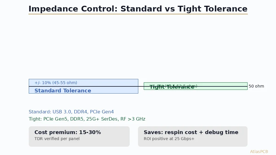
Standard ±10% impedance tolerance is sufficient for most digital designs operating below 5 Gbps, including USB 3.0, HDMI 1.4, and basic DDR4 interfaces. Switch to ±5% tight tolerance when your design operates above 10 Gbps (PCIe Gen5, DDR5, 25G+ SerDes), uses RF frequencies above 3 GHz, or when your signal integrity simulation shows margin loss at ±10% variation. The cost premium for tight tolerance is typically 15-30% — primarily driven by per-panel TDR verification and tighter etch process control.
30-Second Decision: Which Tolerance Do You Need?
| Your Interface / Application | Recommended Tolerance | Why |
|---|---|---|
| USB 2.0 / SPI / I2C | No impedance control needed | Signal speeds well below transmission line threshold |
| USB 3.0 / HDMI 1.4 / DDR4 | ±10% standard | Adequate margin at these data rates |
| PCIe Gen4 / 10GbE / DDR4-3200+ | ±10% (verify with simulation) | Usually sufficient but simulate to confirm |
| PCIe Gen5 / 25G SerDes / DDR5 | ±5% tight tolerance | Reflection budget requires tighter control |
| 56G PAM4 / 112G SerDes | ±5% with comprehensive TDR | Every dB of return loss matters |
| RF 1-3 GHz (WiFi, BLE, GPS) | ±7% or ±10% | Moderate Dk variation acceptable |
| RF 3-28 GHz (5G, radar) | ±5% on Rogers/PTFE | Phase consistency critical |
| RF >28 GHz (mmWave, E-band) | ±3-5% with material characterization | Extreme Dk stability required |
If your design falls in the ±10% column and you specify ±5%, you are paying 15-30% more for capability you do not need. Conversely, if your 25 Gbps SerDes link barely closes timing at nominal impedance in simulation, specifying only ±10% is a gamble that often results in expensive respins.
What Actually Changes Between ±10% and ±5% in Manufacturing
The specification difference sounds small — 5 percentage points. But the manufacturing implications are substantial because tighter tolerance demands changes across the entire fabrication process, not just a final measurement step.
Etch Process Control
At ±10% tolerance, standard spray etching with periodic bath monitoring produces acceptable impedance variation across most panel positions. The etch rate varies naturally across a panel — edges etch faster than center positions due to solution flow dynamics — and this variation falls within the ±10% window for most practical trace widths above 4 mil.
Achieving ±5% requires significantly tighter etch control. In our production line, this means slower etch speeds (reducing throughput by approximately 20%), more frequent etchant concentration monitoring (every 30 minutes versus every 2 hours), and sometimes restricting panel utilization to avoid the highest-variation edge positions. The etch bias — the difference between artwork dimension and actual etched trace width — must be characterized and compensated to within ±0.3 mil instead of the ±0.7 mil acceptable for standard tolerance.
Dielectric Thickness Control
Impedance is a function of trace width, dielectric thickness, and dielectric constant. For ±10% overall impedance tolerance, standard prepreg thickness variation (typically ±10-15% on thin prepregs) is acceptable when combined with reasonable etch control. For ±5% overall, the dielectric thickness contribution must be controlled more tightly — requiring prepreg incoming inspection, press pressure calibration verification, and sometimes selecting specific prepreg lots with measured thickness closer to nominal.
Our process engineers track pressed dielectric thickness on cross-section coupons from every impedance-controlled lot. For tight-tolerance jobs, we correlate this data with the actual TDR measurements to maintain a predictive model that catches drift before it produces out-of-spec panels.
IMPEDANCE SPECIALISTS
±5% Impedance with TDR Data on Every Panel
Per-panel coupon measurement, not sampled. Cpk > 1.33 on production data. TDR report included with every shipment.

The Real Cost Breakdown: Where the Premium Goes
Engineers often assume tight tolerance costs dramatically more because it sounds like a premium capability. The actual cost structure is more nuanced:
Direct Cost Additions for ±5% (compared to ±10% baseline)
| Cost Factor | Impact | Typical Premium |
|---|---|---|
| Per-panel TDR measurement | Labor + equipment time | $2-4 per panel |
| Etch process slow-down | 20% throughput reduction on etch line | 5-10% of total board cost |
| Prepreg inspection/selection | Incoming inspection time | $0.50-1 per panel |
| Higher scrap rate | 5-8% panels outside ±5% vs 1-2% outside ±10% | 3-6% of total cost |
| Coupon area on panel | Reduces usable panel area by 3-5% | 3-5% material cost |
| Total typical premium | 15-30% |
For a standard 6-layer impedance-controlled board (100x100mm, 100-piece order), the difference might be:
- ±10%: $12-18 per board
- ±5%: $15-23 per board
The absolute dollar difference is modest for prototype and low-volume orders. At production volumes (1000+), the percentage premium actually shrinks because the fixed measurement costs are amortized across more panels.
When Tight Tolerance Saves Money Overall
Counterintuitively, specifying ±5% can reduce total project cost when:
Avoiding respins: If your 25 Gbps channel simulation shows 15% margin at nominal impedance, a ±10% board has a meaningful probability of failing validation — requiring a $5,000-20,000 respin cycle. The $300 premium for tight tolerance on 100 prototype boards eliminates this risk.
Reducing debug time: SI engineers spend hours hunting signal integrity issues. When impedance is guaranteed within ±5%, they can eliminate one major variable during debug — saving engineering time worth far more than the board premium.
First-pass yield in production: For high-volume products with tight eye diagram margins, boards at the edges of ±10% tolerance may fail production test. Specifying ±5% improves production test yield, offsetting the board cost premium.
COST OPTIMIZATION
Get Pricing for Both Tolerances — Compare Before Committing
Upload your design and we quote both standard and tight tolerance options with exact pricing. No obligation to choose the premium option.
Compare Impedance Pricing ›Application-Specific Guidance: Real Design Scenarios
High-Speed Digital (PCIe Gen5, DDR5, 56G SerDes)
Modern high-speed digital interfaces operate with extremely tight timing budgets. A PCIe Gen5 link at 32 GT/s has approximately 15.5 ps of unit interval — meaning every source of jitter and reflection matters. Impedance variation directly creates reflections that consume this budget.
At 32 GT/s, a 5% impedance mismatch produces approximately -26 dB return loss at the discontinuity. At 10% mismatch, return loss degrades to -20 dB. For a typical PCIe Gen5 channel budget of -15 dB return loss, a single 10% impedance discontinuity consumes a significant portion of your allocation. When you have multiple via transitions, connector interfaces, and trace impedance variation all contributing, ±5% board impedance is often the minimum that keeps the channel compliant.
For DDR5 at 4800-6400 MT/s, the dual-rank topology with stub lengths makes impedance control critical on both signal and reference planes. We routinely see DDR5 designs fail first-pass validation when fabricated at ±10% tolerance and pass reliably at ±5%.
RF and Microwave (5G, Radar, Satellite Communications)
RF applications present a different challenge — impedance variation affects both return loss and insertion loss phase. A transmission line with ±10% impedance variation produces standing waves that create ripple in the frequency response. For narrowband filters or matching networks, this ripple can shift passband center frequency enough to degrade system performance.
For designs operating above 6 GHz on Rogers or PTFE materials, we recommend ±5% minimum with additional emphasis on Dk tolerance of the laminate material itself. Rogers RO4350B specifies Dk = 3.48 ±0.05, which is already tight — but the fabrication process (etch variation, prepreg resin content) adds additional impedance variation on top of the material tolerance.
Our RF production maintains Cpk > 1.5 on 50-ohm microstrip impedance for Rogers builds, meaning our actual impedance variation is typically within ±3-4% even when specified at ±5%. This additional margin helps RF designs that are sensitive to phase consistency across antenna array elements.
Mixed-Signal and Cost-Optimized Approaches
For boards with both high-speed and standard digital interfaces, the most cost-effective approach is layer-specific tolerance specification:
- Layers 1, 3 (high-speed SerDes routing): ±5% tight tolerance
- Layers 2, 5 (power planes): No impedance requirement
- Layers 4, 6 (standard digital, low-speed): ±10% standard tolerance
This mixed specification allows the manufacturer to focus tight process control on critical layers while processing other layers with standard workflow. The resulting cost lands between full ±10% and full ±5%, typically achieving 85-90% of the tight-tolerance benefit at 60-70% of the premium.
ENGINEERING REVIEW
Not Sure Which Tolerance You Need? Our Engineers Can Advise.
Submit your stackup and we will recommend standard vs tight tolerance for each layer based on your signal speeds and interface requirements.
Get Stackup Recommendation ›How to Specify Impedance Tolerance in Your Fab Drawing
Your fabrication drawing should clearly state:
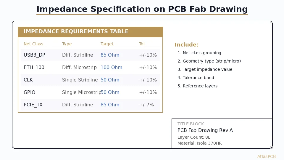
- Target impedance values for each controlled trace type (e.g., “50 ohm single-ended, 100 ohm differential”)
- Tolerance for each: “±5%” or “±10%” — do not assume the manufacturer will default to what you need
- Coupon requirement: “TDR verification coupon required on every panel” for tight tolerance, or “process controlled” for standard
- Reference: which IPC-2141 or specific impedance formula/methodology applies
- Measurement deliverable: “TDR report required with shipment” if you need the verification data
Missing any of these items creates ambiguity that results in either the manufacturer choosing the cheapest interpretation (±10%, no coupon) or quoting conservatively (charging for ±5% verification you may not need).
Summary: Decision Framework
Choose ±10% when your design has adequate signal integrity margin in simulation (>25% timing margin at nominal), operates below 10 Gbps, or you are cost-sensitive and willing to accept slightly higher risk of impedance-related issues.
Choose ±5% when data rates exceed 10 Gbps, RF frequencies exceed 3 GHz, simulation margin is thin (<20% at nominal), or the cost of a potential respin exceeds the impedance tolerance premium across your order quantity.
The decision should be engineering-driven, not habit-driven. Too many engineers default to ±10% because “it has always worked” — then spend weeks debugging SI issues on their first 25 Gbps design. Equally, specifying ±5% on a 100 MHz microcontroller board wastes money without benefit.
ATLASPCB
Impedance Controlled PCB — Both Tolerances, One Manufacturer
Standard ±10% and tight ±5% from the same production line. Per-panel TDR verification. Cpk data available. 1-30 layer capability with Rogers, FR-4, and hybrid stackups.
Upload Design for Quote ›
Reviewed by AtlasPCB Engineering Team — 15+ years in advanced PCB fabrication for RF, HDI, and rigid-flex applications.
Related Reading:
About AtlasPCB — We specialize in complex PCB manufacturing for HDI, RF, and high-reliability applications. Explore our impedance-controlled PCB manufacturing, or get an Megtron 6 & 7 low-loss PCB manufacturing . Every order includes free engineering review. Get your quote.
Reviewed by AtlasPCB Engineering Team — IPC-certified manufacturing specialists with 15+ years of production experience in HDI, RF, and high-reliability PCB fabrication. Content based on factory floor data and real customer design reviews.
Frequently Asked Questions
What is the cost difference between ±10% and ±5% impedance control?
Does JLCPCB offer ±5% impedance control?
When does ±10% impedance tolerance cause signal integrity problems?
How do manufacturers verify tight impedance tolerance?
Can I mix ±10% and ±5% tolerances on the same board?
- impedance controlled PCB manufacturer
- impedance control
- PCB stackup
- controlled impedance
- high-speed PCB