· Sophia Reyes · Engineering · 10 min read
PCB DFM Check for Impedance-Controlled Designs
Standard DFM checks miss impedance-specific issues that cause first-article failures. This guide covers the complete pre-submission verification workflow for controlled-impedance boards — from stackup validation to etch compensation verification — with the exact parameters your fab drawing must specify.
Quick Answer
Impedance-controlled PCBs fail first-article at 3x the rate of standard boards, primarily due to incomplete fab drawing specifications rather than fabrication errors. The critical items most engineers omit: reference layer assignment for each impedance line, dielectric thickness tolerance (not just target), Dk value at operating frequency (not 1 MHz catalog value), and whether etch compensation should target nominal or worst-case impedance. A proper DFM check for impedance boards requires validating these specifications before submission.
The 30-Second Decision
| DFM Checkpoint | Must Specify | Common Omission | Failure Mode |
|---|---|---|---|
| Reference layer | Which ground/power plane | ”50 ohm” without layer ref | Wrong trace geometry |
| Dielectric Dk | Value at operating freq | 1 MHz catalog value used | Impedance off by 5-12% |
| Etch compensation | Manufacturer to optimize | Fixed trace width locked | Post-etch impedance drift |
| Coupon location | Panel edge vs inboard | Not specified | Non-representative measurement |
| Tolerance band | ±5% or ±10% with basis | Unstated or assumed | Over/under-engineered |
Why Standard DFM Checks Miss Impedance Issues
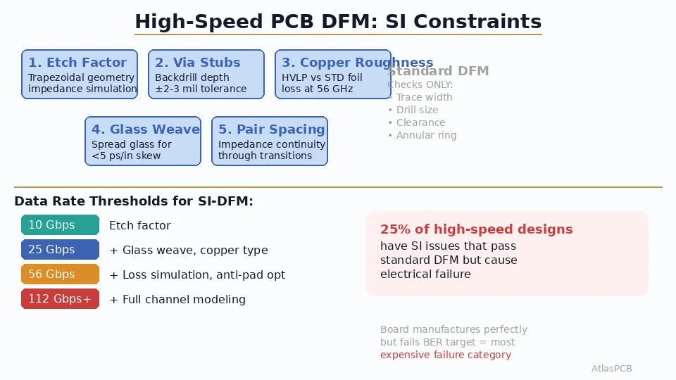
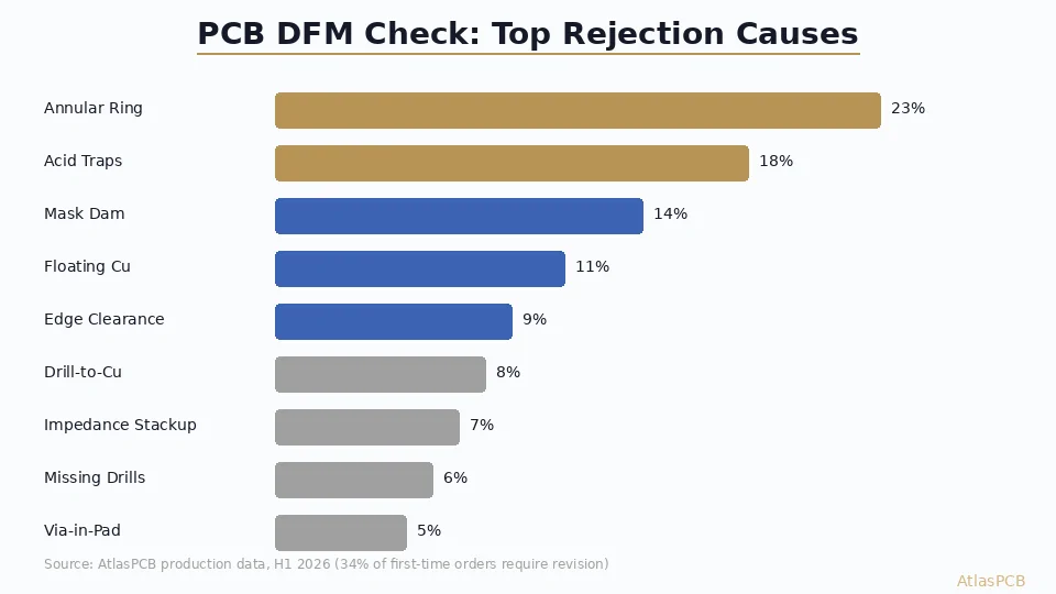
Most PCB DFM tools — whether your EDA’s built-in checker or the manufacturer’s automated Gerber import — validate mechanical rules: minimum trace/space, drill sizes, annular ring, solder mask clearance. These tools have no concept of impedance requirements because impedance depends on the interaction between trace geometry, dielectric properties, and stackup construction — information that lives in fab notes, not Gerber data.
In our facility, we track DFM rejection categories monthly. Impedance-controlled boards submitted by experienced engineers (defense, telecom, medical device companies) still arrive with specification gaps approximately 25% of the time. For general hardware startups and first-time RF designers, the rate exceeds 60%. The resulting back-and-forth adds 3-7 days to delivery, with each revision cycle costing both engineering time and opportunity cost.
The fundamental issue is that impedance is a DERIVED property. Unlike trace width (directly measurable in Gerber data) or drill diameter (explicitly called out in drill files), impedance emerges from the combination of trace width, dielectric thickness, dielectric constant, copper thickness after plating, and etch profile shape. Missing or ambiguous specification of ANY of these inputs produces incorrect impedance on the finished board.
PRE-SUBMISSION REVIEW
Submit Your Stackup for Impedance Validation Before Ordering
Send your fab drawing and stackup requirements. We'll verify manufacturability and return validated trace widths based on our actual material Dk data within 24 hours.
Submit for Review ›
The Complete Impedance DFM Specification Checklist
Every impedance-controlled fab drawing must include these items. Omitting any single element introduces ambiguity that the manufacturer must resolve — either by asking (adding days) or by assuming (risking incorrect fabrication).
Stackup Definition (non-negotiable):
The stackup table must specify the exact layer sequence with copper weights, dielectric materials, and target thicknesses. A properly specified stackup defines which layers are signal, ground, and power, along with the dielectric material between each pair. For impedance-controlled designs, the critical addition is specifying dielectric thickness TOLERANCE — not just the target value. A spec stating “4 mil prepreg” is ambiguous; “4 mil ±0.5 mil prepreg, 1080 glass style” is actionable.
Each prepreg or core material should include the glass style (1080, 2116, 7628) because resin content directly affects Dk. Two different glass styles at the same thickness can produce Dk values differing by 0.2-0.3 — enough to shift impedance by 3-5%.
Impedance Table (the critical document):
Your fab drawing’s impedance table should look like this:
| Net Class | Type | Target (ohm) | Tolerance | Signal Layer | Reference Layer | Notes |
|---|---|---|---|---|---|---|
| USB_DP/DN | Differential | 90 | ±5% | L1 | L2 (GND) | Edge-coupled microstrip |
| ETH_TX+/- | Differential | 100 | ±5% | L3 | L2 (GND), L4 (GND) | Broadside-coupled stripline |
| RF_ANT | Single-ended | 50 | ±5% | L1 | L2 (GND) | Microstrip, GCPW optional |
| CLK_100M | Single-ended | 50 | ±10% | L3 | L2 (GND) | Standard tolerance acceptable |
Every row specifies the geometry type (microstrip, stripline, coplanar), signal and reference layers explicitly, and whether the tolerance is ±5% or ±10%. This eliminates the most common source of impedance DFM failures.
Five DFM Errors That Kill Impedance-Controlled First Articles
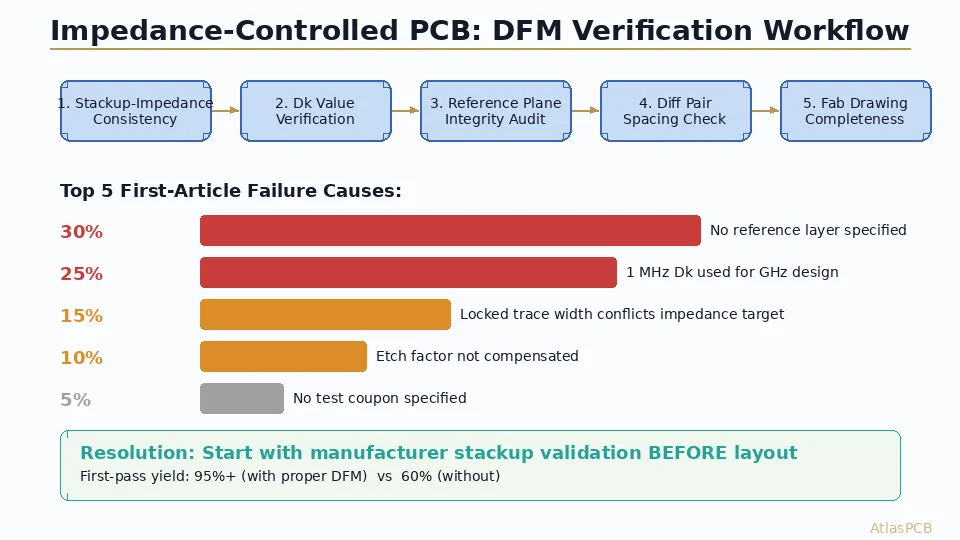
Based on our production rejection data, these five specification errors account for 85% of impedance-controlled first-article failures:
Error 1: Specifying impedance without reference layer assignment. The same 50-ohm requirement produces radically different trace widths depending on which ground plane is the reference and the dielectric thickness between them. We see this on approximately 30% of incoming impedance-controlled designs. The fix is trivial: add one column to your impedance table specifying the reference layer.
Error 2: Using 1 MHz Dk values for GHz-frequency designs. Material datasheets often lead with the 1 MHz Dk value because it’s the IPC test standard (IPC-TM-650 2.5.5.9). But Dk decreases with frequency — standard FR-4 drops from approximately 4.5 at 1 MHz to 4.2 at 2 GHz to 4.0 at 10 GHz. Designing a 5 GHz impedance structure using Dk = 4.5 produces trace widths that are 8-12% too narrow, resulting in impedance 5-8% above target. Always specify the Dk value at your operating frequency, or reference the material’s high-frequency datasheet.
Error 3: Locking trace widths in Gerber data while also specifying impedance targets. When your Gerber files contain fixed trace widths AND your fab notes specify impedance targets, any conflict forces the manufacturer to choose which specification to violate. The correct approach: design to target impedance geometry, but indicate in fab notes that “trace width may be adjusted by manufacturer to achieve target impedance.” This allows etch compensation without requiring a complete redesign.
Error 4: Ignoring etch factor impact on impedance. Standard chemical etching removes copper laterally as well as vertically (undercut). A 5-mil target trace on 1oz copper typically etches to 4.0-4.3 mil at the base depending on the etch process. This trapezoidal cross-section produces different impedance than the rectangular cross-section assumed by simple impedance calculators. A 1-mil width reduction on a 50-ohm microstrip increases impedance by approximately 3-4 ohms (6-8%). Your manufacturer’s etch compensation table accounts for this — but only if they’re allowed to adjust trace width.
Error 5: No test coupon specification. Without explicit test coupon requirements, the manufacturer may place coupons at panel edges (where dielectric thickness varies due to panel bow) or omit them entirely on small batches. Specify: “Impedance test coupon required, matching production trace geometry, located within the active panel area.” For ±5% tolerance work, request that the coupon location be documented in the fabrication report.
ENGINEERING SUPPORT
We Catch These Errors Before They Hit Production
Our DFM team reviews impedance specifications against actual process capabilities. No generic automated check — real engineer review of your specific stackup.
Our DFM Process ›The Pre-Submission Verification Workflow
Before submitting your impedance-controlled design to any manufacturer, follow this systematic verification workflow. Each step catches a specific class of error that automated DFM tools cannot detect.
Step 1: Stackup-to-Impedance Consistency Check. Open your EDA tool’s impedance calculator (Altium’s stackup manager, KiCad’s PCB Calculator, or standalone tool like Saturn PCB Toolkit). Input your ACTUAL stackup values — not generic defaults. Verify that the calculated trace widths match what’s in your layout within ±0.5 mil. If they don’t match, your layout was designed to a different stackup than what you’re specifying. This single check catches 40% of impedance DFM errors.
Step 2: Dk Value Verification. Look up your specified material’s Dk at your operating frequency. Cross-reference this against the value in your impedance calculation. If using a manufacturer’s stackup library (Altium’s stackup wizard, for example), verify the Dk values aren’t stale 1 MHz catalog numbers. For Rogers materials, use the Dk values from the “High Frequency Laminate” datasheet, not the “Standard Properties” summary.
Step 3: Reference Plane Integrity Audit. In your layout, check every impedance-controlled trace for ground plane continuity beneath it. Any via, slot, or copper void in the reference plane disrupts the impedance. This is particularly common around BGA breakouts where power vias punch through the ground plane directly under signal traces. A single via hole in the reference plane can create a local impedance spike of 10-20%.
Step 4: Differential Pair Spacing Verification. For differential pairs, verify that the pair-to-pair spacing in your layout matches your impedance calculation assumptions. Many EDA tools default to a specific coupling gap, but layout constraints (BGA pitch, via rows) force different spacing in practice. Odd-mode impedance is extremely sensitive to coupling gap — a 1-mil spacing change on a 4-mil gap alters differential impedance by 5-8%.
Step 5: Fab Drawing Completeness Audit. Before submission, verify your fab drawing includes all items from the checklist above. Missing any single element is grounds for a quality-conscious manufacturer to pause fabrication and request clarification — or for a less careful shop to make assumptions.
Working with Your Manufacturer: The Impedance-First Approach
The most efficient workflow for impedance-controlled designs reverses the typical ordering process. Instead of finalizing your layout, generating Gerbers, and then submitting to a manufacturer, work the stackup and impedance requirements FIRST.
Contact your manufacturer before finalizing the PCB layout. Provide your impedance requirements (types, targets, tolerances), layer count and thickness constraints, material preference or requirements, and operating frequency range. A manufacturer with proper impedance capability will return a validated stackup based on their current material inventory, target trace widths calculated from their measured Dk data, and any constraints or recommendations (glass style, resin content, lamination requirements).
Design your layout to THESE trace widths and stackup values. When you submit Gerbers, the impedance will be correct by construction rather than by luck. This approach eliminates first-article iterations and gets boards right the first time — we see first-pass yield above 95% for customers who follow this workflow versus 60-65% for those who design in isolation and submit complete Gerbers cold.
IMPEDANCE EXPERTISE
Start with Stackup Validation — Not Gerber Submission
Tell us your impedance requirements before you route. We'll provide validated stackup and trace widths from our actual material data. Design right the first time.
Request Stackup Validation ›Fab Drawing Template: What a Complete Impedance Specification Looks Like
For reference, here’s the minimum information a well-specified impedance-controlled fab drawing contains beyond standard mechanical requirements:
Material specification: IT-180A (or equivalent, Tg 180C minimum), Dk 4.2 ±0.15 at 1 GHz, Df under 0.020 at 1 GHz.
Stackup: Full layer table with copper weights, dielectric materials, target thicknesses with tolerances, and glass styles.
Impedance requirements: Table format with net class, geometry type, target impedance, tolerance, signal layer, reference layer(s), and any special notes (coplanar gap, edge-coupled spacing).
Manufacturing notes: “Manufacturer to adjust trace width for impedance. Etch compensation per manufacturer’s process. Test coupon required per IPC-2141, located in active panel area. TDR report to be included with shipment.”
Acceptance criteria: “Impedance verification per IPC-TM-650 2.5.5.7 Method C (TDR). All values within specified tolerance band. Report to include raw TDR trace data.”
This level of specification eliminates ambiguity and gives your manufacturer everything needed to fabricate correct impedance on the first attempt. It takes 30 minutes to write properly but saves weeks of iteration.
ATLASPCB
Get Your Impedance Right the First Time
Upload your design files and impedance requirements. Our engineers validate your stackup against our process capabilities and return confirmed trace geometries within 24 hours.
Upload Design ›
Reviewed by AtlasPCB Engineering Team — 15+ years in advanced PCB fabrication for RF, HDI, and rigid-flex applications.
Related Reading:
About AtlasPCB — We specialize in complex PCB manufacturing for HDI, RF, and high-reliability applications. Explore our RF and high-frequency PCB services, impedance-controlled PCB manufacturing, or get an free engineering DFM review . Every order includes free engineering review. Get your quote.
Reviewed by AtlasPCB Engineering Team — IPC-certified manufacturing specialists with 15+ years of production experience in HDI, RF, and high-reliability PCB fabrication. Content based on factory floor data and real customer design reviews.
Frequently Asked Questions
What is the most common DFM error on impedance-controlled PCBs?
Should I specify trace width in my impedance-controlled fab drawing?
How do I verify my stackup is manufactureable before submitting?
What Dk value should I specify — 1 MHz or operating frequency?
How often do impedance-controlled PCBs fail first-article?
- PCB DFM check
- impedance controlled PCB manufacturer
- PCB stackup design guide
- RF PCB design and manufacturing
- controlled impedance