· Sophia Reyes · Engineering · 11 min read
224G SerDes PCB Design
Building PCBs for 224 Gbps PAM4 SerDes pushes every fabrication parameter to its limit. This guide covers the material selection (Megtron 7, Tachyon 100G), stackup design, copper roughness requirements, and manufacturing process constraints for next-generation AI interconnect boards operating beyond 56 GHz Nyquist.
Quick Answer
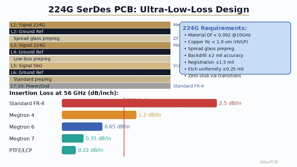
224G PAM4 SerDes requires PCB channel insertion loss below 1.0 dB/inch at 56 GHz (Nyquist frequency), demanding ultra-low-loss laminates (Df < 0.002 at 10 GHz), HVLP copper foil (Rz < 1.0 um), spread-glass prepreg, and backdrill accuracy within ±2 mils. Standard FR-4 materials fail catastrophically at these frequencies — even Megtron 6 class materials are marginal. Production requires Megtron 7, Panasonic Megtron R-5785N, or Rogers/Isola equivalents (Tachyon 100G, I-Speed Ultra) with fabrication processes that maintain theoretical material performance through manufacturing.
The 224G Challenge: Where Material Physics Meets Manufacturing Reality
The transition from 112G to 224G PAM4 SerDes represents a fundamental inflection point in PCB fabrication. At 112G (28 GHz Nyquist), Megtron 6 class materials with VLP copper deliver adequate performance for 6-8 inch channels. At 224G (56 GHz Nyquist), those same materials produce channels that cannot be equalized — the loss at Nyquist exceeds what even the most advanced DSP can recover. The PCB industry must deploy materials and processes that were exotic prototyping exercises just two years ago as volume production requirements.
The core problem is loss accumulation. At 56 GHz, every material imperfection, every rough copper grain boundary, every glass fiber in your prepreg contributes measurable insertion loss. A channel budget that had 5 dB of margin at 112G rates may show negative margin at 224G on identical physical geometry — because loss scales with frequency in a manner that compounds faster than linear. Dielectric loss increases proportionally with frequency (doubling from 28 to 56 GHz), but conductor roughness loss increases approximately as the square root of frequency, and radiation loss from discontinuities increases with the cube of frequency.
The result: what worked at 112G does not scale to 224G by simply choosing “better material.” The entire fabrication approach — material selection, copper specification, stackup architecture, via design, and process control — must be co-optimized as a system.
NEXT-GEN FABRICATION
224G-Capable PCB Manufacturing
Megtron 7 processing, HVLP copper, spread glass, and ±2mil backdrill accuracy. Validated channel loss data available for your design review.
Discuss Your 224G Design ›
Material Selection: The Df < 0.002 Threshold
For 224G PAM4 channels operating at 56 GHz Nyquist, the material dissipation factor threshold is approximately Df = 0.002 at 10 GHz for channels exceeding 4 inches. Below this threshold, the channel loss remains within the equalization capability of current-generation SerDes DSP (typically 35-40 dB of CDR/DFE/FFE capability). Above Df 0.002, even the best equalization cannot recover signal quality for typical switch-board channel lengths.
The material landscape for 224G-capable PCBs:
| Material | Dk (10 GHz) | Df (10 GHz) | Df (56 GHz) | 224G Viability | Relative Cost |
|---|---|---|---|---|---|
| Standard FR-4 (Tg170) | 4.2-4.5 | 0.018-0.022 | 0.025+ | Not viable | 1.0x |
| Mid-loss (Megtron 4 class) | 3.8-4.0 | 0.006-0.008 | 0.010-0.012 | Not viable | 2.5x |
| Low-loss (Megtron 6 class) | 3.6-3.7 | 0.003-0.004 | 0.005-0.006 | Marginal (<3”) | 4-5x |
| Ultra-low-loss (Megtron 7) | 3.3-3.4 | 0.001-0.0015 | 0.002-0.003 | Yes (8-10”) | 7-10x |
| Tachyon 100G (Isola) | 3.0-3.2 | 0.0012-0.0015 | 0.002-0.003 | Yes (8-10”) | 8-12x |
| AP-99X (AGC) | 3.2-3.3 | 0.0010-0.0012 | 0.0015-0.002 | Yes (10-12”) | 10-15x |
| PTFE (modified) | 2.1-2.2 | 0.0008-0.001 | 0.001-0.0015 | Best loss | 15-20x |
The material choice for 224G is not simply “pick the lowest Df” — manufacturing processability matters enormously. Megtron 7 retains FR-4-like processing (standard drill, plate, laminate), making it the practical choice for volume AI switch boards. PTFE offers lower loss but requires specialized drilling, plasma treatment, and bonding techniques that reduce yield and increase cost. For most 224G applications, Megtron 7 or Tachyon 100G provides the optimal balance of electrical performance and manufacturing feasibility.
Copper Roughness: The Dominant Loss Mechanism at 56 GHz
At 224G PAM4 operating frequencies, conductor roughness loss exceeds dielectric loss as the primary loss mechanism for ultra-low-loss materials. This creates a counterintuitive situation: switching from Megtron 6 to Megtron 7 material while keeping standard copper foil delivers only 30-40% of the expected loss improvement — because the copper roughness loss has not changed and now dominates the total.
The physics: current at 56 GHz is confined to a skin depth of approximately 0.28 um. Standard electrodeposited copper has treated-side roughness (Rz) of 5-8 um — meaning the current must navigate over peaks and valleys that are 20-30x deeper than the current penetration depth. The effective path length increase from this roughness adds loss according to the Huray or Hammerstad-Jensen models, typically contributing 0.3-0.5 dB/inch at 56 GHz on standard foil.
Copper foil options for 224G:
| Foil Type | Rz (um) | Additional Loss at 56 GHz | Availability | Processing Notes |
|---|---|---|---|---|
| Standard ED (STD) | 5-8 | +0.4-0.6 dB/inch | Universal | Standard process |
| Reverse-treated (RTF) | 3-5 | +0.25-0.35 dB/inch | Common | Standard process |
| Very-low-profile (VLP) | 1.5-3 | +0.10-0.18 dB/inch | Common | Slight peel strength reduction |
| Hyper-VLP (HVLP) | 0.8-1.5 | +0.04-0.08 dB/inch | Specialized | Requires careful handling |
| Ultra-flat (UHVLP) | 0.4-0.8 | +0.02-0.04 dB/inch | Limited | Adhesion challenges |
For 224G channels, HVLP is the minimum viable copper type. The difference between VLP and HVLP at 56 GHz is 0.06-0.10 dB/inch — over an 8-inch channel, that is 0.5-0.8 dB of channel loss. In a budget where total channel loss cannot exceed 30-35 dB (the equalization limit), every 0.5 dB matters enormously.
The manufacturing challenge with HVLP: smoother copper has lower peel strength (adhesion to laminate). Standard ED copper achieves 6-8 lb/inch peel strength; HVLP drops to 3-4 lb/inch. This reduced adhesion makes the copper more susceptible to delamination during thermal cycling, via drilling, and reflow soldering. Fabricators must adjust process parameters — reduced lamination pressure, modified microetch chemistry, and controlled drilling entry speed — to prevent adhesion failures. Not all manufacturers have validated their processes for HVLP foil on ultra-low-loss materials.
HVLP COPPER EXPERTISE
Validated HVLP Process for Ultra-Low-Loss Boards
Our process engineers have characterized HVLP copper on Megtron 7 with measured peel strength and insertion loss data. First-pass yield above 82% on 224G-class designs.
View High-Speed Capabilities ›Stackup Architecture for 224G Channels
The stackup for 224G-capable boards differs from conventional high-speed designs in several critical ways. Signal layer-to-reference distance must be tightly controlled (typically 3.0-3.5 mil on ultra-low-loss prepreg) for impedance targets. Every prepreg layer adjacent to a 224G signal must use spread glass to eliminate fiber weave skew. The stackup must minimize the number of layer transitions (via stubs are essentially prohibited at these frequencies), often requiring carefully planned signal layer assignments that avoid unnecessary transitions.
A representative 16-layer stackup for a 224G AI switch application:
| Layer | Function | Material | Copper | Notes |
|---|---|---|---|---|
| L1 | Signal (224G) | Megtron 7 core 3.0mil | HVLP 0.5oz | Primary SerDes routing |
| L2 | Ground reference | — | STD 1oz | Continuous plane, minimal splits |
| L3 | Signal (224G) | Spread glass prepreg 3.2mil | HVLP 0.5oz | Secondary high-speed |
| L4 | Ground reference | — | STD 1oz | Continuous plane |
| L5 | Signal (56G/PCIe) | Low-loss prepreg 3.5mil | VLP 0.5oz | Mid-speed SerDes |
| L6 | Ground reference | — | STD 1oz | |
| L7 | Power (0.85V core) | Standard prepreg | STD 2oz | Power delivery plane |
| L8 | Ground reference | — | STD 1oz | Power/signal boundary |
| L9 | Ground reference | — | STD 1oz | Power/signal boundary |
| L10 | Power (1.2V, 3.3V) | Standard prepreg | STD 2oz | Secondary power |
| L11 | Ground reference | — | STD 1oz | |
| L12 | Signal (56G/PCIe) | Low-loss prepreg 3.5mil | VLP 0.5oz | Mid-speed SerDes |
| L13 | Ground reference | — | STD 1oz | |
| L14 | Signal (224G) | Spread glass prepreg 3.2mil | HVLP 0.5oz | Secondary high-speed |
| L15 | Ground reference | — | STD 1oz | |
| L16 | Signal (224G) | Megtron 7 core 3.0mil | HVLP 0.5oz | Primary SerDes routing |
Note the asymmetric material usage: only signal layers carrying 224G traffic use ultra-low-loss material and HVLP copper. Power planes and mid-speed signals use standard materials at a fraction of the cost. This hybrid material approach reduces total stackup material cost by 40-50% compared to all-ultra-low-loss construction, with negligible electrical penalty because power and ground planes do not carry high-frequency signal current.
Via Design: Zero-Stub Transitions at 56 GHz
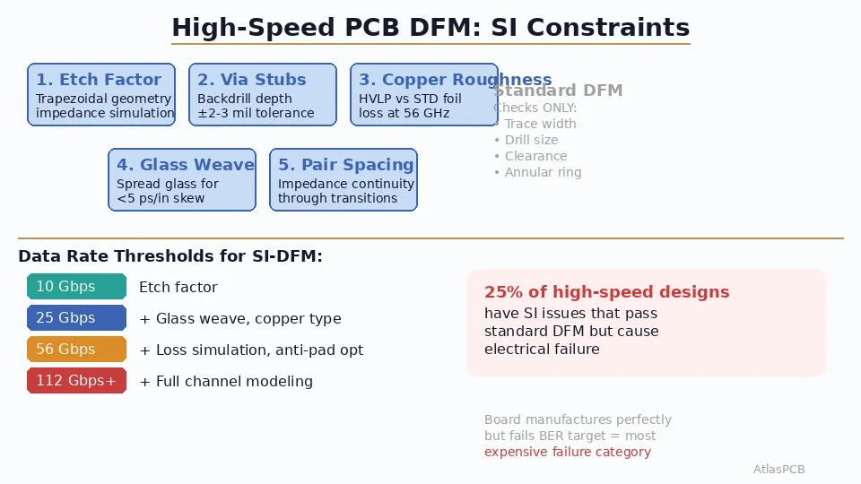
At 224G PAM4 frequencies, via stubs are essentially unacceptable. Even a 3-mil residual stub creates a resonant notch that impacts the 56 GHz Nyquist region. The practical options for layer transitions in 224G designs are:
Blind/buried vias (preferred): Laser-drilled microvias or mechanically-drilled blind vias terminate exactly at the target layer with zero stub. This is the recommended approach for all 224G signal transitions. The cost premium of blind/buried via construction (HDI processing) is justified at these data rates because the alternative — backdrilling with ±2 mil tolerance — still leaves stub residual that may impact performance.
Precision backdrilling (acceptable with caveats): For transitions in conventional through-hole sections of the board, backdrilling to within ±2 mils of the signal layer is viable for 224G if the remaining stub is less than 3 mils. This requires: x-ray depth measurement feedback, controlled-depth spindle with impedance-sensing endpoint detection, and 100% inspection of backdrill depth on production panels. Not all fabricators can achieve ±2 mil consistently.
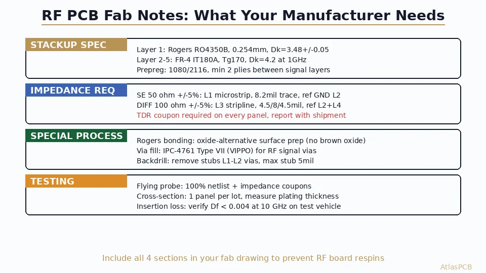
Via optimization (mandatory regardless of approach): The via anti-pad, pad size, and surrounding ground via arrangement must be impedance-optimized. A standard 20-mil via pad with 30-mil anti-pad creates a capacitive discontinuity that reflects 56 GHz signal energy. Optimized designs use reduced pad size (12-14 mil), enlarged anti-pad (35-40 mil), and tightly coupled ground return vias (6-8 ground vias within 30 mils of the signal via) to maintain 50-ohm impedance through the entire via transition.
From our fabrication data, the via transition loss contribution at 56 GHz:
| Via Configuration | Insertion Loss at 56 GHz | Return Loss | Manufacturing Complexity |
|---|---|---|---|
| Standard via, 8mil stub | -3.5 to -5.0 dB | -8 dB | Standard |
| Backdrilled ±4mil, 4mil residual | -1.5 to -2.5 dB | -12 dB | Medium |
| Backdrilled ±2mil, 2mil residual | -0.8 to -1.2 dB | -16 dB | High |
| Blind via (zero stub) | -0.3 to -0.6 dB | -20 dB | HDI process |
| Optimized blind + ground vias | -0.2 to -0.4 dB | -23 dB | HDI + precision |
Manufacturing Process Requirements
Producing 224G-capable boards requires process capabilities that go beyond standard PCB manufacturing. Here are the critical process parameters and what they demand from the fabrication facility:
Lamination profile control: Ultra-low-loss materials like Megtron 7 have narrower lamination process windows than standard FR-4. The resin flow must be precisely controlled to achieve target dielectric thickness (±0.3 mil versus ±0.5 mil for standard boards). Over-flow reduces dielectric thickness and increases impedance; under-flow creates resin-starved voids that increase loss. Our lamination presses use thermocouple monitoring at multiple panel positions with closed-loop temperature control to maintain ±2°C uniformity across the press opening.
Registration accuracy: At 3/3 mil trace/space on 0.5oz HVLP copper with tight impedance requirements, layer-to-layer registration must be within ±2 mils. Standard registration (±3-4 mil) is inadequate because registration error directly affects the trace-to-reference distance and thus impedance. We achieve ±1.5 mil registration using pin-lamination with optical alignment verification at each layer.
Etch uniformity: For 3.5 mil trace widths on HVLP copper, etch variation must be within ±0.3 mil across the panel. Standard spray etch with single-side nozzles achieves ±0.5-0.7 mil variation. We use horizontal etch with oscillating spray bars and in-line optical measurement to maintain ±0.25 mil uniformity — critical for delivering consistent impedance across all board positions in the panel.
Drill quality: Mechanical drills for via holes in ultra-low-loss laminate must avoid delamination at the entry and exit surfaces. HVLP copper’s lower adhesion makes it more susceptible to drill-exit burring. We use entry/exit material specifically selected for low-loss laminate processing and reduce spindle speed by 15-20% compared to standard FR-4 parameters.
AI INFRASTRUCTURE PCB
Building the Next Generation of AI Interconnect?
We manufacture 224G-class PCBs for AI switch, NIC, and optical transceiver applications. Megtron 7, HVLP copper, and validated channel loss data included with every quote.
AI Data Center Application Context
The primary driver for 224G SerDes PCB technology is AI training and inference cluster interconnect. Current-generation AI accelerators (GPU and custom ASICs) use 112G PAM4 SerDes for chip-to-chip and chip-to-optical module connections. The next generation (shipping 2026-2027 from major silicon vendors) doubles to 224G PAM4 to meet the bandwidth demands of larger AI models requiring faster inter-GPU communication.
A typical AI switch board carries 128 lanes of SerDes at 224G, delivering 3.2 Tbps of aggregate bandwidth through a single chip package. The PCB must route these 128 lanes (64 differential pairs transmit + 64 receive) from the switch ASIC BGA to front-panel optical module cages — distances of 6-10 inches depending on switch architecture. At this channel length and data rate, the PCB is the limiting factor in system bandwidth. Material and manufacturing choices directly determine whether the system achieves its target BER of 1e-15 after FEC.
The economic reality: a single 224G AI switch board contains $800-1500 of PCB material and processing cost, but it enables a switch platform worth $30,000-80,000 that serves an AI cluster worth millions. The PCB cost premium for 224G-capable fabrication is a small fraction of system value, making it one of the highest-ROI investments in the entire data center bill of materials.
ATLASPCB
Your AI Hardware Needs Ultra-Low-Loss PCBs — We Deliver Them
From switch boards to NIC modules to optical transceiver substrates. Megtron 7, Tachyon 100G, and HVLP copper with validated 56 GHz insertion loss measurements on production panels.
Start Your AI PCB Project ›
Reviewed by AtlasPCB Engineering Team — 15+ years in advanced PCB fabrication for RF, HDI, and rigid-flex applications.
Related Reading:
About AtlasPCB — We specialize in complex PCB manufacturing for HDI, RF, and high-reliability applications. Explore our HDI PCB manufacturing capabilities, RF and high-frequency PCB services, or get an impedance-controlled PCB manufacturing . Every order includes free engineering review. Get your quote.
Reviewed by AtlasPCB Engineering Team — IPC-certified manufacturing specialists with 15+ years of production experience in HDI, RF, and high-reliability PCB fabrication. Content based on factory floor data and real customer design reviews.
Frequently Asked Questions
What PCB materials support 224G PAM4 SerDes?
Why is copper roughness critical for 224G PCB channels?
What channel length is achievable at 224G PAM4?
Can standard PCB manufacturers produce 224G-capable boards?
How does 224G PCB cost compare to standard server boards?
- RF PCB design and manufacturing
- impedance controlled PCB manufacturer
- HDI PCB manufacturer
- PCB stackup design guide
- China RF PCB manufacturer