· Marcus Lin · Engineering · 9 min read
5G Antenna PCB Fabrication
Practical fabrication guide for 5G mmWave antenna PCBs covering Rogers RO4350B hybrid stackups, via fence design rules for surface wave suppression, patch element manufacturing tolerances, and the production challenges that determine whether your antenna array meets pattern specifications.
Quick Answer
5G mmWave antenna PCBs at 28/39 GHz require Rogers RO4350B or equivalent low-loss laminates with tightly controlled Dk (3.66 +/-0.05), via fence spacing under lambda/10 (under 1mm at 28 GHz), patch element dimensional tolerance of +/-0.5mil, and hybrid stackup construction that bonds RF layers to FR-4 support structure without delamination at reflow temperatures.
Quick Reference: 5G mmWave Antenna PCB Specifications
| Parameter | 28 GHz (n257/n258) | 39 GHz (n260) |
|---|---|---|
| Substrate | Rogers RO4350B (Dk 3.66) | Rogers RO4350B or RT5880 |
| Substrate thickness | 0.254mm (10mil) or 0.508mm (20mil) | 0.254mm (10mil) preferred |
| Patch element size | ~2.7 x 2.7mm | ~1.9 x 1.9mm |
| Element spacing | 5.0-5.4mm (0.47-0.50 lambda) | 3.5-3.8mm |
| Via fence pitch | 0.4-0.5mm | 0.3-0.4mm |
| Via drill diameter | 0.2mm (laser) or 0.25mm (mechanical) | 0.15-0.2mm (laser preferred) |
| Trace width tolerance | +/-0.5mil (LDI required) | +/-0.5mil (LDI required) |
| Impedance | 50 ohm +/-5% | 50 ohm +/-5% |
| Surface finish | ENIG (uniform, non-oxidizing) | ENIG |
These are manufacturing parameters, not design guidelines. Your antenna simulation determines the element geometry; these specs define what the fabrication process must achieve to realize your design.
Why mmWave Antennas Push PCB Fabrication to Its Limits
Antenna PCB fabrication at 28-39 GHz operates in a regime where manufacturing tolerances directly determine whether the antenna works at all. Unlike lower-frequency RF where a few percent dimensional variation causes minor gain reduction, at mmWave frequencies the same percentage error can shift the antenna completely off-band or destroy the array pattern.
Consider the math: at 28 GHz, the guided wavelength in RO4350B (Dk 3.66) is approximately 5.6mm. A resonant patch is roughly half a wavelength — about 2.7mm square. The bandwidth of a patch antenna on 10mil substrate is approximately 3-4% (840 MHz - 1.1 GHz). A +/-2mil (50um) fabrication error on that 2.7mm patch shifts the resonant frequency by approximately 200-300 MHz — enough to move the center frequency outside the allocated 5G band.
This is why mmWave antenna PCBs demand manufacturing capability that most PCB shops cannot deliver. Standard etching processes with +/-1.5mil tolerance (adequate for digital PCBs) produce antennas that are detuned by design. Only facilities with LDI exposure, controlled-rate spray etching, and in-process dimensional verification at the element level can reliably produce mmWave antenna arrays.
In our RF production line, we measure patch element dimensions on every panel using automated optical inspection (AOI) calibrated to +/-0.3mil resolution. Panels where any element exceeds +/-0.5mil from target are reworked or scrapped. Our typical first-pass yield on 28 GHz antenna arrays is 88-92% — meaning 8-12% of panels require attention. This yield rate is already considered excellent for mmWave fabrication and reflects the inherent difficulty of the process.
CHINA RF PCB MANUFACTURER
mmWave Antenna PCB Fabrication
Rogers RO4350B hybrid stackups with LDI exposure and element-level dimensional verification. Production-proven for 28/39 GHz 5G antenna arrays with +/-0.5mil tolerance.
Get RF PCB Quote ›
Hybrid Stackup Design: Rogers RF Layers on FR-4 Structure
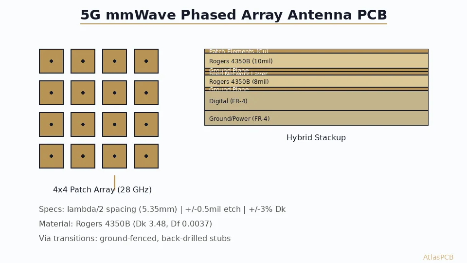
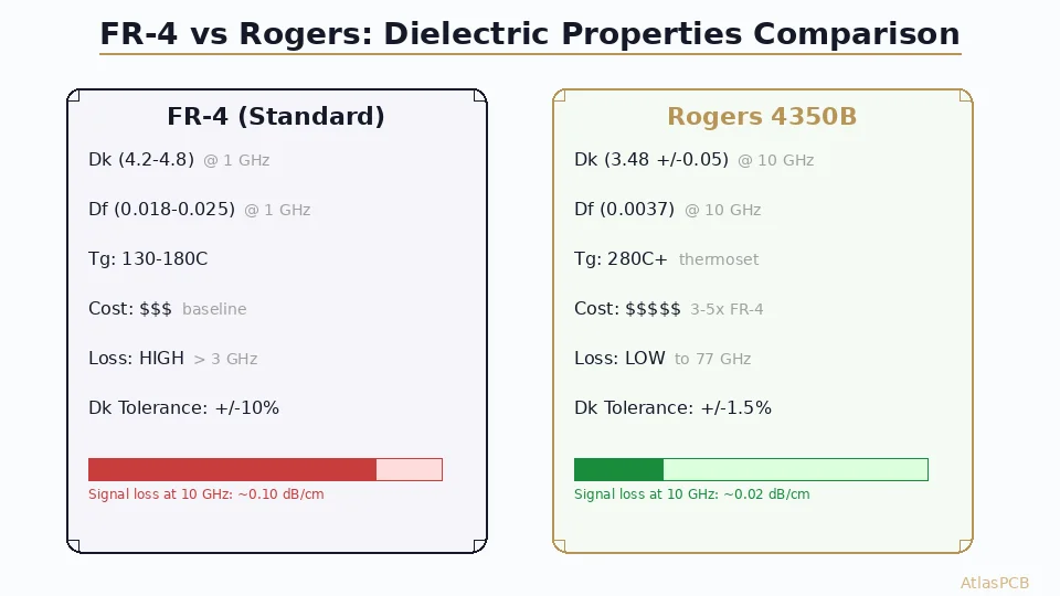
All-Rogers stackups are technically ideal but economically punishing. A 6-layer all-Rogers board costs 5-8x more than an equivalent FR-4 board and offers no benefit on the non-RF layers that carry power distribution and digital control signals. The solution universally adopted by 5G equipment manufacturers is the hybrid stackup: Rogers for RF layers, FR-4 for everything else.
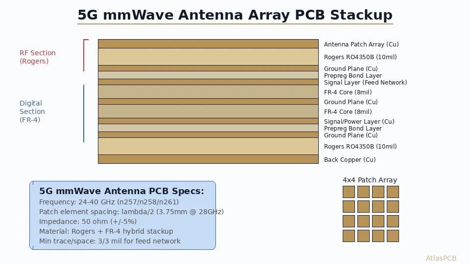
Typical 6-Layer Hybrid Stackup for 28 GHz Antenna Module:
- L1: Antenna elements (1oz copper on RO4350B)
- Substrate: RO4350B, 0.254mm (10mil)
- L2: Antenna ground plane (1oz copper)
- Bondply: Rogers 4450F, 0.1mm
- L3: Feed network / beamforming (1oz copper on RO4350B)
- Substrate: RO4350B, 0.254mm
- L4: RF ground (0.5oz copper)
- Prepreg: Standard FR-4 prepreg, 2x2116
- L5: Power distribution (1oz copper)
- Core: FR-4 core, 0.4mm
- L6: Digital control / I2C / SPI (1oz copper)
The critical fabrication challenge is the Rogers-to-FR-4 bonding interface. Standard FR-4 prepreg does not bond reliably to RO4350B because the surface chemistry is different. We use Rogers 4450F bondply (a thermoset adhesive film with matched Dk) or Isola 185HR low-flow prepreg for this interface. The lamination profile must be carefully controlled — too much pressure squeezes adhesive into the ground plane area, creating Dk variations under the antenna elements. Too little pressure leaves voids that fail in thermal cycling.
Our process uses a two-stage lamination: first, the Rogers layers are bonded together with 4450F bondply in a dedicated RF layup. Then this RF subassembly is bonded to the FR-4 structure in a second press cycle using modified lamination parameters (lower pressure, longer dwell time at Tg). This adds manufacturing time but ensures both the RF performance and the mechanical integrity of the joint.
Via Fencing: The Manufacturing Challenge Nobody Talks About
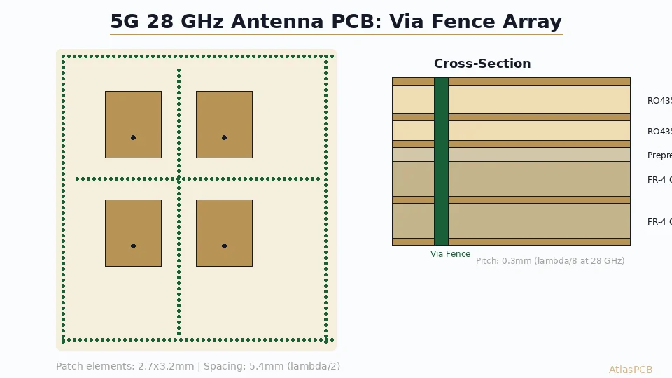
Via fencing (rows of plated vias surrounding antenna elements and transmission lines) is essential for mmWave performance but creates significant fabrication challenges. At 28 GHz, the required via pitch (under 0.5mm) means you are placing vias with only 0.25-0.3mm of laminate between them. At 39 GHz, the pitch drops to 0.3-0.4mm with even less material between vias.
The problems this creates in fabrication:
Drill wander and registration: At 0.2mm drill diameter with 0.5mm pitch, the drill hit must be positioned within +/-0.05mm of the target location. Any larger offset and the via-to-via copper spacing becomes insufficient for reliable plating isolation. We use CCD camera alignment on each panel and spindle calibration at 4-hour intervals to maintain positional accuracy.
Resin starvation in dense via fields: When you drill hundreds of closely-spaced holes through a thin laminate, the copper plating process must fill the via barrels while maintaining uniform thickness. Dense via fields draw more plating current per unit area, potentially creating thin spots in nearby traces. Our plating rectifier programming accounts for via density maps extracted from the drill file — areas with dense fencing receive modified current ramping.
Coverlay/prepreg flow into via fields: During subsequent lamination cycles (in the hybrid stackup), resin from prepreg or bondply can flow into unfilled vias. For via fencing, the vias must either be completely filled and planarized before the next lamination step, or the press parameters must minimize resin flow. We use via filling with copper paste followed by surface grinding for antenna PCBs — adding cost but ensuring that via fencing maintains its electromagnetic function.
RF PCB DESIGN AND MANUFACTURING
Via Fencing Done Right
Our RF production line handles via fence pitches down to 0.3mm with filled and planarized vias. CCD-aligned drilling and density-compensated plating ensure consistent performance across the antenna aperture.
RF PCB Capabilities ›Surface Finish Selection for mmWave Antennas
Surface finish choice at mmWave frequencies is not merely a solderability decision — it directly affects antenna performance because the skin depth at 28 GHz is only about 0.4 micrometers. The surface finish IS the conductor as far as the RF signal is concerned.
ENIG (Electroless Nickel Immersion Gold): The standard choice for mmWave antenna PCBs. The 3-5um nickel layer provides a uniform, non-oxidizing surface that maintains consistent conductivity over the antenna lifetime. The thin gold layer (0.05-0.1um) prevents nickel oxidation. Drawback: nickel has higher resistivity than copper, adding approximately 0.3-0.5 dB loss per wavelength at 28 GHz compared to bare copper. This is acceptable for most designs.
Immersion Silver: Lower loss than ENIG (silver conductivity is 6% higher than copper) but tarnishes over time if not properly sealed. Suitable for designs where loss budget is extremely tight, but requires controlled storage environment and short shelf life before assembly. Not recommended for antenna products with long storage requirements.
OSP (Organic Solderability Preservative): Lowest cost, lowest loss (bare copper with thin organic coating). However, the organic coating degrades over time and provides no oxidation protection in humid environments. The antenna performance may change over product lifetime as the copper surface oxidizes. Only suitable for immediate-assembly high-volume production with controlled shelf life.
Our recommendation for most 5G antenna applications: ENIG with 3-5um nickel thickness. The slightly higher loss is offset by consistent long-term performance, excellent solderability for component attachment, and compatibility with aluminum wire bonding if the antenna module includes active ICs.
5G ANTENNA PCB FABRICATION
Production-Ready mmWave Antenna Arrays
From prototype to volume production — Rogers hybrid stackups, LDI exposure for +/-0.5mil element tolerance, filled via fencing, and ENIG finish optimized for 28/39 GHz performance.
Upload Antenna Design ›Testing and Verification: Proving Your Antenna PCB Works
Unlike digital PCBs where electrical testing (open/short) and impedance coupons verify fabrication quality, antenna PCBs require additional verification to confirm that the manufactured board will produce the intended radiation pattern.
What we verify on every mmWave antenna panel:
- Patch element dimensions (AOI): +/-0.5mil from Gerber target
- Via fence position accuracy: +/-0.05mm from design
- Substrate thickness (cross-section on coupon): +/-8% from nominal
- Impedance (TDR on test coupon): 50 ohm +/-5%
- Surface finish thickness (XRF): Ni 3-5um, Au 0.05-0.1um
What the customer should verify (antenna-level testing):
- Return loss (S11) at target frequency band
- Radiation pattern (gain, beamwidth, sidelobe level)
- Element-to-element coupling (S21 between adjacent ports)
- Scan impedance variation for phased arrays
We provide dimensional inspection reports with every mmWave antenna order, including statistical analysis of element dimensions across the panel. This data allows the antenna engineer to correlate any measured pattern anomalies with fabrication variations — critical for diagnosing whether a performance issue is a design problem or a manufacturing issue.
ATLASPCB
Building a 5G Antenna Module? Start with the Right PCB.
Rogers hybrid stackups, element-level AOI verification, filled via fencing at sub-0.5mm pitch. Our RF production line is purpose-built for mmWave antenna fabrication from prototype through volume production.
Get 5G Antenna PCB Quote ›
Reviewed by AtlasPCB Engineering Team — 15+ years in advanced PCB fabrication for RF, HDI, and rigid-flex applications.
Related Reading:
About AtlasPCB — We specialize in complex PCB manufacturing for HDI, RF, and high-reliability applications. Explore our RF and high-frequency PCB services, or get an Rogers RO4350B PCB manufacturing . Every order includes free engineering review. Get your quote.
Reviewed by AtlasPCB Engineering Team — IPC-certified manufacturing specialists with 15+ years of production experience in HDI, RF, and high-reliability PCB fabrication. Content based on factory floor data and real customer design reviews.
Frequently Asked Questions
Why is Rogers RO4350B preferred for 5G antenna PCBs?
What via fence pitch is needed for 28 GHz antenna PCBs?
How tight must patch element dimensions be at mmWave frequencies?
Can FR-4 be used for 5G antenna PCBs?
What does a hybrid stackup for 5G antenna PCB look like?
- 5G antenna PCB
- mmWave PCB fabrication
- Rogers 4350B
- RF PCB manufacturer
- antenna array