· Marcus Lin · Engineering · 12 min read
5G mmWave Antenna Array PCB: Material Selection, Via Strategy, and Manufacturing for 24-40 GHz
A manufacturing-focused guide to PCB design for 5G mmWave antenna arrays operating at 24-40 GHz. Covers Rogers vs PTFE material selection, via fence isolation requirements, feed network loss budgets, and the fabrication tolerances that determine array radiation pattern integrity.
Quick Answer
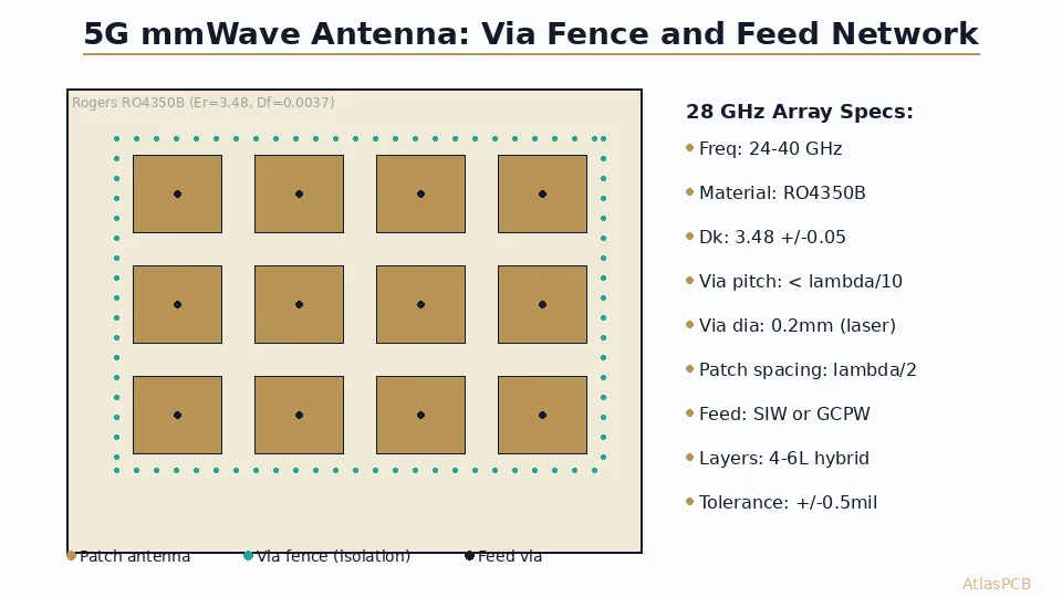
5G mmWave antenna arrays at 24-40 GHz require Rogers RO4350B or RO3003 substrates with tightly controlled dielectric thickness (+/-0.5 mil), via fencing at lambda/10 pitch for surface wave suppression, and fabrication tolerances below +/-1 mil on patch dimensions to maintain beam pattern integrity. The critical manufacturing challenge is achieving consistent Dk across the antenna aperture — a 2% Dk variation shifts beam pointing by 1-3 degrees at 28 GHz.
Quick Decision: Material Selection for mmWave Antenna Arrays
| Operating Band | Frequency | Recommended Material | Feed Loss (dB/cm) | Key Consideration |
|---|---|---|---|---|
| n257/n258 | 24.25-29.5 GHz | Rogers RO4350B | 0.025 | FR-4 compatible process |
| n260/n261 | 37-40 GHz | Rogers RO3003 | 0.012 | Lower loss for long feeds |
| n259 | 39.5-43.5 GHz | Rogers RO3003 or RT/duroid 5880 | 0.009 | PTFE needed above 40 GHz |
| E-band backhaul | 71-86 GHz | RT/duroid 5880 | 0.006 | Specialized PTFE process |
The Manufacturing Challenge at mmWave Frequencies
Designing a phased array antenna at 28 GHz and actually manufacturing it with consistent performance across production lots are fundamentally different problems. In simulation, your patch antenna resonates at exactly 28.0 GHz with 15 dBi gain and -20 dB sidelobe level. In production, the question becomes: can your PCB manufacturer hold the dimensional tolerances that keep 64 patch elements in phase across a 50mm aperture?
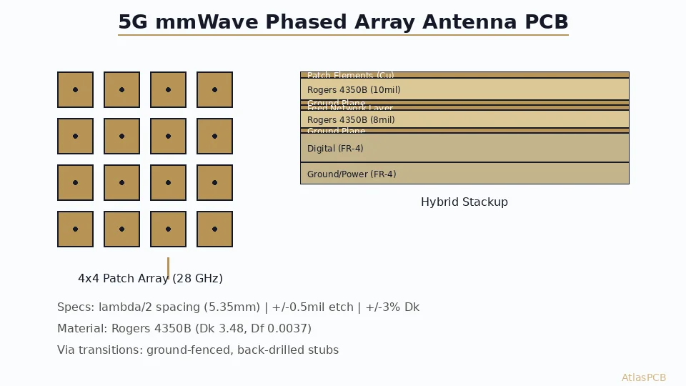
At 28 GHz, a half-wavelength in Rogers RO4350B (Dk=3.48) is approximately 2.87mm. The patch dimension that determines resonant frequency is typically 2.6-2.8mm. A +/-1 mil (25 um) etch tolerance on this dimension shifts the resonant frequency by approximately 50 MHz — about 0.2% of center frequency. For a narrowband patch with 3-5% bandwidth, this shift is manageable. But when you have 64 elements that must maintain phase coherence across the array, even small random dimensional variations degrade the composite beam pattern.
Our experience fabricating mmWave antenna arrays for 5G base station customers has shown that three manufacturing parameters dominate array performance: copper feature accuracy, dielectric thickness uniformity, and via placement precision. Standard PCB fabrication tolerances (+/-3 mil etch, +/-10% dielectric thickness) are catastrophically inadequate. You need a manufacturer operating at +/-1 mil etch tolerance, +/-0.5 mil dielectric thickness control, and +/-2 mil via registration — and you need them to maintain these tolerances across the entire antenna aperture, not just at coupon measurement points.
Material Selection: Rogers RO4350B vs RO3003 vs PTFE
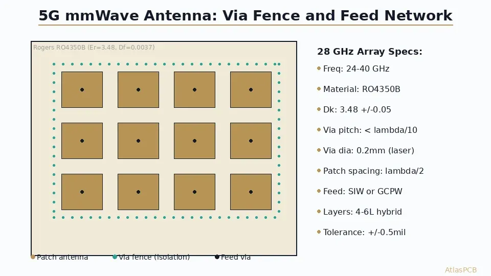
The material choice for a mmWave antenna array depends on three interrelated factors: feed network length, operating frequency, and manufacturing complexity tolerance. There is no single “best” material — only the right material for your specific array architecture.
Rogers RO4350B (Dk=3.48, Df=0.0037 @ 10 GHz) remains the workhorse for 24-30 GHz antenna arrays where the corporate feed network length is under 100mm. Its primary advantage is process compatibility with standard FR-4 fabrication: same drill bits, same etch chemistry, same press temperatures (with minor profile adjustments). In our production, we achieve Dk variation of +/-0.03 across a standard 18x24 inch panel, which translates to less than 0.5 degree phase error between elements at the panel edges — acceptable for most 5G base station requirements.
The limitation of RO4350B becomes apparent in two scenarios. First, when the feed network exceeds 100mm total path length, the cumulative insertion loss at 28 GHz (approximately 2.5 dB for a 100mm corporate feed) starts to consume your link budget. Second, at frequencies above 35 GHz, the Df of 0.0037 contributes increasingly to total loss, and you begin to see measurable performance degradation in the outer elements of large arrays that have the longest feed paths.
Rogers RO3003 (Dk=3.00, Df=0.0013 @ 10 GHz) offers 60% lower loss per unit length than RO4350B, making it the preferred choice for larger arrays (128+ elements) at 28 GHz or any array operating above 35 GHz. The lower Dk also means larger patch dimensions (easier to etch accurately) and wider traces for the same impedance (better yield). The manufacturing tradeoff: RO3003 is a ceramic-filled PTFE material that requires modified processing. Standard oxide treatments do not work for bonding; instead, we use plasma treatment or sodium naphthalenide preparation to achieve adequate peel strength at the copper-dielectric interface.
RT/duroid 5880 (Dk=2.20, Df=0.0009 @ 10 GHz) is the lowest-loss commercial option, reserved for E-band (71-86 GHz) and applications where every 0.1 dB of feed loss matters. The very low Dk means patch elements are physically larger (easier fabrication) but the PTFE substrate is soft, dimensionally unstable during handling, and requires completely specialized processing. Lead times are 2-3x longer than RO4350B designs.
5G ANTENNA MANUFACTURING
mmWave Antenna Arrays with Verified Phase Matching
We maintain Rogers RO4350B and RO3003 inventory specifically for 5G antenna production. Every antenna panel undergoes cross-section verification for dielectric thickness and etch uniformity measurement across the array aperture.
View RF Antenna Capabilities ›
Via Fence Design: The Key to Element Isolation
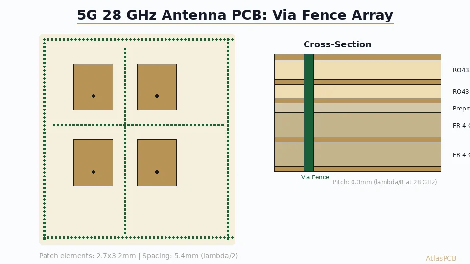
Surface wave suppression is not optional at mmWave frequencies — it is a fundamental requirement for achieving specified array performance. Without via fencing between antenna elements, surface waves propagating along the substrate couple energy between adjacent patches, creating three problems: elevated sidelobe levels, scan blindness at certain steering angles, and element-to-element mutual coupling that degrades active impedance matching.
The physics is straightforward: at 28 GHz in RO4350B (Dk=3.48), the TM0 surface wave propagates with a wavelength of approximately 5.7mm along the substrate. Any distance between elements that is a significant fraction of this wavelength allows efficient coupling. The via fence acts as a corrugated metal wall, creating a cutoff condition for surface wave propagation between elements.
Via fence design rules for 28 GHz arrays:
The required via pitch is lambda_surface/10 or less to maintain effective suppression. At 28 GHz in RO4350B, this means via center-to-center spacing of approximately 0.55mm maximum. For 39 GHz arrays, the spacing tightens to 0.38mm. These pitches are achievable with laser-drilled microvias (0.1-0.2mm diameter) but impossible with standard mechanical drilling.
Via diameter should be as large as practical given the pitch constraint. Larger vias have lower inductance and provide better suppression of the evanescent field behind the fence. Our standard process for 28 GHz antenna vias uses 0.2mm laser-drilled holes on 0.5mm pitch, with copper-filled vias for structural reliability through thermal cycling.
The fence must extend from the top ground plane to the bottom ground plane (or full substrate thickness) to be effective. Blind vias that terminate in the middle of the stackup create a gap in the fence that surface waves can leak through. For multi-layer antenna stackups, ensure the via fence connects all ground layers continuously.
Our production data on 5G antenna panels shows that proper via fencing improves element isolation from -15 dB (no fence) to -30 dB or better at 28 GHz. This 15 dB improvement directly translates to sidelobe level performance — the difference between a -20 dB SLL specification pass and a -12 dB SLL failure.
Feed Network Design and Loss Management
The corporate feed network that distributes the signal from a single input to 64 or 256 antenna elements is often the performance-limiting component in a mmWave array. Every power divider junction, every 90-degree bend, and every millimeter of transmission line adds loss. At 28 GHz, the total feed network loss for a 64-element array with corporate binary feed is typically:
| Component | Loss per stage | Stages (64 elements) | Total |
|---|---|---|---|
| Wilkinson divider (per split) | 0.15-0.25 dB | 6 | 0.9-1.5 dB |
| Transmission line (avg path) | 0.025 dB/mm (RO4350B) | 40mm avg | 1.0 dB |
| 90-degree bends | 0.05-0.10 dB each | 4-6 average | 0.2-0.6 dB |
| Via transitions (layer change) | 0.10-0.20 dB each | 1-2 | 0.1-0.4 dB |
| Total feed loss | 2.2-3.5 dB |
This 2-3.5 dB loss represents power that never reaches the antenna elements — it is dissipated as heat in the feed network. For a 64-element array with 30 dBm total input power, this means 0.5-1.0W of thermal dissipation in the feed network alone, concentrated in a small area that can create thermal gradients affecting Dk stability.
From a manufacturing perspective, the feed network imposes the tightest trace width tolerance requirement. A 50-ohm transmission line on 5-mil RO4350B substrate has a microstrip width of approximately 10.5 mil. A +/-1 mil width variation changes impedance by +/-5 ohms, creating reflections at every point where the width deviates. These distributed reflections accumulate along the feed path and can shift the effective phase at each element by 5-10 degrees at 28 GHz — directly degrading beam steering accuracy.
In our facility, we achieve feed network trace width consistency of +/-0.7 mil across the antenna aperture by using laser direct imaging (LDI) rather than phototool-based imaging. LDI eliminates the dimensional distortion that occurs in film phototools due to temperature and humidity variation during exposure. For antenna customers, we also perform in-process width measurement at multiple points across the panel to verify uniformity before proceeding to etch.
RF PCB DESIGN AND MANUFACTURING
Antenna Array PCBs with Sub-Mil Feature Accuracy
Laser Direct Imaging, cross-section verified dielectric thickness, and per-panel TDR impedance reports. We support full production volumes for 5G mmWave antenna modules with documented traceability for telecom qualification.
Stackup Architecture for 5G Antenna Modules
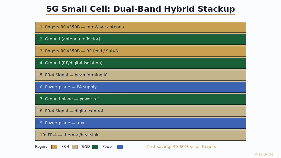
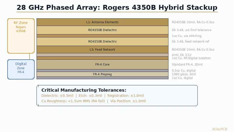
A typical 5G mmWave antenna module combines the antenna array with beamforming ICs, power management, and digital control in a single PCB. This requires a hybrid stackup that places Rogers material on the antenna layers while using standard FR-4 for the digital and power sections.
A production-proven 6-layer hybrid stackup for a 28 GHz 4x4 antenna module:
- L1: Rogers RO4350B (5 mil) — Antenna patches + feed network (50 ohm microstrip)
- Bond ply: Rogers 4450F prepreg (4 mil) — Low-loss bonding layer
- L2: Copper — Solid ground plane (antenna reference + feed network reference)
- Core: FR-4 (15 mil) — Mechanical support core
- L3: Copper — Power distribution (RFIC bias, LDO outputs)
- Prepreg: FR-4 2116 (4 mil)
- L4: Copper — Digital control signals (SPI, GPIO, I2C to beamformer ICs)
- Core: FR-4 (15 mil)
- L5: Copper — Ground plane (digital reference)
- Prepreg: FR-4 2116 (4 mil)
- L6: Copper — BGA pads for module attachment / heat sink interface
The critical manufacturing requirement is the L1-L2 dielectric thickness control. The 5-mil Rogers layer determines the microstrip impedance of the entire feed network and the resonant frequency of every patch element. In our process, we achieve +/-0.3 mil thickness tolerance on this layer by using precision-thickness Rogers cores (not pressed prepreg) and verifying with cross-section measurement on the first panel of each production lot.
The Rogers-to-FR-4 transition at the L2/Core boundary must be managed carefully. CTE mismatch between Rogers (CTE-z = 32 ppm/C) and FR-4 (CTE-z = 50-70 ppm/C) creates stress during thermal cycling that can propagate cracks at the interface. We address this by using Rogers 4450F bondply (CTE-matched to RO4350B) at the transition and maintaining symmetric stackup construction.
Manufacturing Tolerance Budget for 28 GHz Arrays
For engineers specifying tolerances in their fab drawings, here is our recommended tolerance budget that we have validated across production volumes of 5G antenna panels:
| Parameter | Tolerance | Impact if Exceeded |
|---|---|---|
| Patch dimension (length/width) | +/-1.0 mil (25 um) | 50 MHz/mil frequency shift |
| Feed trace width | +/-0.7 mil (18 um) | 5 ohm/mil impedance change |
| Dielectric thickness (antenna layer) | +/-0.5 mil (12 um) | 2% impedance shift per 0.5 mil |
| Via position (feed via) | +/-2.0 mil (50 um) | Impedance mismatch at feed |
| Via fence pitch uniformity | +/-3.0 mil (75 um) | Degraded isolation locally |
| Copper thickness (antenna layer) | +/-0.2 mil (5 um) | Minor frequency shift |
| Panel-to-panel Dk variation | +/-0.05 (1.4%) | Element phase scatter |
These tolerances are tighter than standard PCB manufacturing but well within capability for a manufacturer with proper process controls and Rogers material experience. The key is communicating these requirements clearly in your fab drawing — do not assume your manufacturer will know which features are antenna-critical without being told.
CHINA RF PCB MANUFACTURER
5G Antenna Production with Full Traceability
We hold +/-1 mil etch tolerance on antenna features, maintain Rogers material inventory for rapid prototyping, and provide cross-section and TDR reports with every antenna array shipment. Supporting production volumes for Tier-1 telecom equipment manufacturers.
Get Antenna PCB Quote ›Summary: Getting mmWave Antenna Arrays into Production
The path from simulated antenna performance to consistent production results at 28-40 GHz requires tight collaboration between RF designer and PCB manufacturer. The material selection determines your loss floor, the via architecture determines your isolation ceiling, and the manufacturing tolerances determine whether your array pattern survives production variation.
Key takeaways for engineers designing 5G mmWave antenna PCBs:
Specify Rogers RO4350B for arrays up to 64 elements at 24-30 GHz with feed networks under 100mm. Move to RO3003 for larger arrays, longer feeds, or operation above 35 GHz. Demand via fencing at lambda/10 pitch with laser-drilled vias connected through all ground layers. Tighten your standard PCB tolerances to +/-1 mil on antenna features and +/-0.5 mil on dielectric thickness. And most critically — choose a manufacturer who routinely processes mmWave antenna designs and can demonstrate tolerance capability with production data, not just datasheet claims.
ATLASPCB
Building a 5G Antenna Module? Start with the Right PCB Partner.
Send us your antenna array Gerbers for a manufacturing feasibility review. We will assess tolerance requirements, recommend material options, and provide production pricing with lead times for your volume requirements.
Submit Antenna Design ›
Reviewed by AtlasPCB Engineering Team — 15+ years in advanced PCB fabrication for RF, HDI, and rigid-flex applications.
Related Reading:
About AtlasPCB — We specialize in complex PCB manufacturing for HDI, RF, and high-reliability applications. Explore our RF and high-frequency PCB services, Rogers RO4350B PCB manufacturing, or get an multilayer PCB fabrication up to 30 layers . Every order includes free engineering review. Get your quote.
Reviewed by AtlasPCB Engineering Team — IPC-certified manufacturing specialists with 15+ years of production experience in HDI, RF, and high-reliability PCB fabrication. Content based on factory floor data and real customer design reviews.
Frequently Asked Questions
What PCB material is best for 28 GHz 5G antenna arrays?
Why are via fences critical in mmWave antenna PCBs?
What fabrication tolerances matter most for 5G antenna PCBs?
Can standard PCB manufacturers fabricate 5G mmWave antenna boards?
How does via fence pitch affect manufacturing cost?
- 5G antenna PCB fabrication
- RF PCB design and manufacturing
- mmWave PCB
- Rogers 4350B stackup
- China RF PCB manufacturer