· AtlasPCB Engineering · Engineering · 11 min read
HDI PCB Cost Optimization: 5 Design Changes That Cut 2+N+2 Pricing by 25-40%
Practical engineering guide to reducing HDI PCB manufacturing cost without sacrificing electrical performance. Covers microvia diameter optimization, staggered vs stacked via strategies, buildup reduction analysis, and panel utilization techniques that our process engineers use to bring customer quotes within budget.
Quick Answer
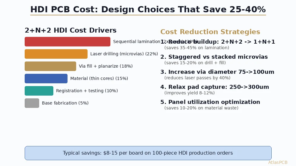
The three largest cost drivers in 2+N+2 HDI boards are sequential lamination (30% of cost), laser drilling (22%), and via fill/planarization (18%). Reducing buildup from 2+N+2 to 1+N+1 saves 35-45% immediately. If 2+N+2 is required, switching from stacked to staggered microvias saves 15-20%, increasing via diameter from 75 to 100 um reduces laser passes by 40%, and optimizing panel utilization saves 10-20% on material cost.
Quick Answer: Where Does HDI Cost Come From?
| Cost Driver | % of HDI Premium | Optimization Available |
|---|---|---|
| Sequential lamination (extra press cycles) | 30% | Reduce buildup layers |
| Laser drilling (microvias) | 22% | Increase diameter, reduce count |
| Via fill + planarization | 18% | Staggered vias, selective fill |
| Thin core material premium | 15% | Standard core where possible |
| Registration + layer alignment | 10% | Relax capture pad tolerance |
| Additional testing/inspection | 5% | Risk-based sampling |
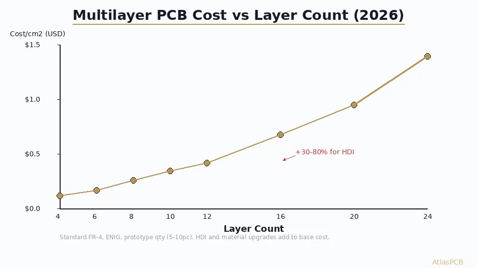
A standard 12-layer board costs roughly $8-12 per piece at 500 units. The same layer count in 2+N+2 HDI construction costs $22-30 — a 2-3x premium driven by the process complexity listed above. But 25-40% of that premium is recoverable through design optimization without sacrificing electrical performance.
The Fundamental Cost Equation
HDI pricing is not a mystery — it follows directly from process steps. Every sequential lamination cycle requires a full press cycle (8-12 hours including setup, press, and cool-down), precise alignment of inner layers to previously-built outer layers, and post-lamination inspection. The key insight for cost optimization is that each buildup layer represents a multiplicative cost step, not an additive one.
Going from a standard through-hole 12-layer board to 1+N+1 (10-layer core with one microvia layer each side) adds roughly one press cycle per side, one laser drill step per side, and one via fill step per side. This translates to approximately 45-65% cost increase over the base through-hole board. Stepping up to 2+N+2 doubles the number of extra process steps, but the cost increase is more than double because each subsequent lamination must align to the previous microvia layer — tightening registration requirements and reducing panel yield.
In our facility, we track the yield impact of each buildup layer. A well-controlled 1+N+1 process achieves 94-96% first-pass panel yield. Adding a second buildup layer (2+N+2) drops this to 88-92% depending on design complexity. That 4-6% yield difference translates directly to cost because rejected panels consume the same material, energy, and processing time as good panels.
Understanding this cost structure is the first step toward optimization: every design choice that eliminates a process step, reduces laser drilling time, or improves yield has a direct and calculable impact on per-board pricing.
HDI PRICING
Get an Itemized HDI Quote with Cost Breakdown
We show exactly which process steps drive your HDI cost — and where design changes can reduce it.
Upload HDI Design ›
Strategy 1: Reduce Buildup — The Biggest Single Savings
The most impactful cost reduction in HDI is also the most obvious: use fewer buildup layers. If your design currently requires 2+N+2 construction, the question to ask is whether the second microvia layer is truly necessary or whether it’s a convenience that could be eliminated with routing optimization.
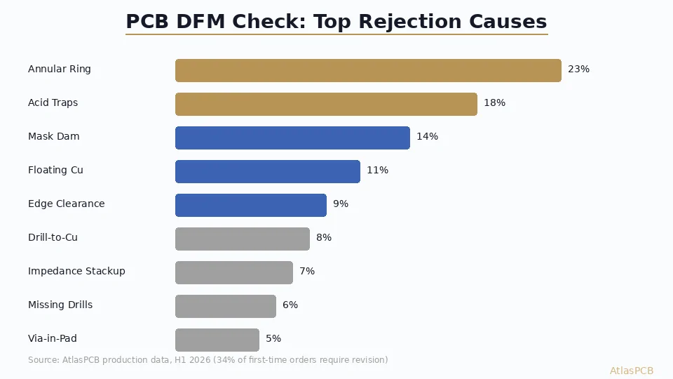
In our DFM reviews, approximately 30% of designs submitted as 2+N+2 can be restructured to 1+N+1 with routing modifications. The most common scenario is a design with one large BGA (0.5mm pitch, 400+ balls) on the top side requiring two microvia layers for escape routing, while the bottom side has only SMT passives that don’t require microvia access at all. In this case, a 1+N+1 or even 1+N+0 buildup (HDI on top side only) achieves the same functionality at 35-45% lower cost.
The engineering work to evaluate this is straightforward: count the routing channels needed to escape your densest BGA and determine whether a single microvia layer provides enough via access. For a 0.65mm pitch BGA, a single microvia layer almost always suffices (escape through first ring of pads via microvia to layer 2, route on layers 2-3, drop to inner layers via buried via). For 0.5mm pitch with 500+ balls, you might need 2 microvia layers on the BGA side but potentially zero on the opposite side.
The savings are dramatic: removing one buildup layer from a 2+N+2 design (going to 2+N+1 or 1+N+2) eliminates one lamination cycle, one laser drill step, one fill/planarize step, and improves yield by 2-3 percentage points. On a 500-piece production order for a 14-layer board, this can save $4,000-7,000 in total manufacturing cost.
Strategy 2: Staggered Microvias Eliminate Fill Requirements
When 2+N+2 construction is genuinely required (both sides need microvia access to inner routing layers), the next optimization target is the via structure. Stacked microvias — where the second-layer via lands directly on top of the first-layer via — require that the first-layer via be filled with conductive paste and planarized flat before the second layer is built. This fill-and-planarize step is expensive: it involves screen-printing conductive paste under vacuum, curing, then grinding/polishing the surface to achieve less than 10 um planarity.
Staggered microvias (where the second-layer via is offset from the first-layer via by the pad diameter) eliminate this fill requirement because the second via lands on solid copper pad rather than on top of a void. The first-layer microvia still exists underneath, but it doesn’t need to be filled — only capped with copper plating during the subsequent lamination cycle.
The cost saving from staggered vs stacked microvias is approximately 15-20% of the HDI cost premium, which translates to $2-4 per board on a typical 12-14 layer 2+N+2 design at 500 pieces. The tradeoff is that staggered vias require larger capture pads (typically 350-400 um diameter vs 250-300 um for stacked), which consumes additional routing space on the microvia layers.
The design decision depends on routing density: if you have available space for the larger pads without losing critical routing channels, staggered vias are essentially free money. Our process engineers routinely evaluate this tradeoff during DFM review and can provide specific pad geometry recommendations that maintain routing viability while enabling the staggered approach.
DESIGN OPTIMIZATION
HDI DFM Review Identifies Cost Reduction Opportunities
Our engineers analyze your HDI design for staggered via candidates, buildup reduction, and yield improvement before quoting.
HDI Manufacturing ›Strategy 3: Optimize Microvia Diameter
Laser drilling is charged by time, and drilling time is a function of via diameter, depth, and quantity. A 75 um microvia through a 60 um dielectric requires 3-4 laser pulses at full power. A 100 um via through the same dielectric needs only 1-2 pulses. For a board with 10,000 microvias (common on dense HDI designs with via-in-pad for fine-pitch BGAs), this difference translates to 40-60% reduction in laser drill time per panel.
The electrical impact of increasing from 75 to 100 um diameter is negligible for most applications. The via parasitic capacitance increases from approximately 0.04 pF to 0.06 pF — a difference that only matters for ultra-high-speed serial links above 56 Gbps or RF circuits above 10 GHz where every fraction of a dB of insertion loss matters. For standard high-speed digital (PCIe Gen4/5, DDR5, USB4), 100 um microvias have no measurable impact on signal integrity.
Beyond the direct laser time saving, larger vias also improve manufacturing yield. The copper plating process deposits copper more uniformly in wider vias, achieving more consistent plating thickness without the voids and thin spots that plague minimum-diameter vias. Our yield data shows a 5-8% improvement in first-pass panel yield when minimum microvia diameter increases from 75 to 100 um — a secondary cost saving that compounds with the direct drilling cost reduction.
The practical recommendation: start your design with 100 um microvias as default, and reduce to 75 um only for specific vias where routing density absolutely demands it (typically the innermost escape ring of 0.4mm pitch BGAs). This mixed approach captures most of the cost benefit while maintaining routing capability where it’s needed most.
Strategy 4: Panel Utilization and Array Optimization
Panel material is a fixed cost that doesn’t scale with board complexity — but it scales inversely with utilization. A poorly optimized array that achieves only 55% panel utilization effectively increases your material cost by 30% compared to a well-optimized array at 75% utilization.
Most engineers leave panelization to the manufacturer, which is fine if your manufacturer actively optimizes for utilization. But many shops simply apply a standard array configuration without exploring alternatives. For rectangular boards that don’t tile efficiently on standard 18x24” panels, consider these approaches:
First, discuss array rotation. A board that achieves 60% utilization in landscape orientation might achieve 72% rotated 90 degrees. Second, for production volumes above 1000 pieces, ask about alternative panel sizes — some HDI lines can run 21x24” or 18x21” panels that might better match your board dimensions. Third, for boards with irregular outlines, tab routing with breakaway tabs allows tighter nesting than standard V-score separation, recovering 8-12% panel area.
In our quoting process, we automatically evaluate 3-5 array configurations and select the option with best utilization for the customer’s volume. For a recent 500-piece HDI order, switching from a standard 2x4 array (62% utilization) to a 3x3 array with rotation (74% utilization) saved $2.10 per board — $1,050 total on the order — with no design changes required from the customer.
Strategy 5: Selective Application of HDI Features
Not every via on an HDI board needs to be a microvia. Many designers apply HDI construction across the entire board when only specific areas (around fine-pitch BGAs, for instance) actually require microvia access. The rest of the board could use standard through-hole vias or buried vias in the core layers without impacting functionality.
The cost optimization here is indirect but significant: reducing total microvia count reduces laser drilling time, and more importantly, reducing the density of microvias in non-critical areas improves yield by reducing the probability of a single defective via causing panel rejection.
A common pattern we see is a design with one high-density FPGA BGA on the top side requiring HDI escape, and 80% of the remaining board area containing standard-pitch connectors, power components, and discrete analog circuits that could use conventional 0.3mm mechanical drills. By confining microvia usage to the BGA fanout zone and using standard vias elsewhere, you reduce total laser-drilled features by 40-60% — a direct per-panel cost reduction and yield improvement.
Our process engineers call this “surgical HDI” — applying high-density features only where the design demands them. During DFM review, we identify vias that are currently specified as microvias but could be replaced with mechanical drills based on their location and the layers they connect. This optimization alone typically saves 8-15% on laser drilling cost.
COST REDUCTION
Let Us Identify Savings in Your HDI Design
Upload your design and we provide a marked-up DFM report showing where cost can be reduced without impacting performance.
Putting It All Together: Combined Savings Example
Consider a real-world scenario: a 14-layer 2+N+2 HDI board, 60x80mm, with two 0.5mm pitch BGAs (one per side), 0.075mm microvias, stacked construction, full via fill. At 500 pieces, initial quote: $28.50 per board.
After DFM optimization applying the strategies above:
- Bottom BGA only needs 1 microvia layer (reduce to 2+N+1): saves $3.20/board
- Top-side stacked vias converted to staggered where possible: saves $1.80/board
- Microvia diameter increased to 100 um except BGA inner ring: saves $1.40/board
- Array re-optimized from 2x4 to 3x3 with rotation: saves $1.60/board
- 35% of vias outside BGA zones converted to mechanical drill: saves $1.10/board
Optimized price: $19.40 per board — a 32% reduction with zero impact on electrical performance verified through post-layout signal integrity simulation.
Total savings on 500-piece order: $4,550. Engineering review time: 4 hours. That’s a return on engineering investment that justifies DFM optimization on essentially every HDI production order.
ATLASPCB
HDI Production? Get a Quote with Optimization Report.
Every HDI quote includes a DFM optimization report identifying cost reduction opportunities. Upload your Gerbers and stackup specification to start.
Get Instant Quote ›
Reviewed by AtlasPCB Engineering Team — 15+ years in advanced PCB fabrication for RF, HDI, and rigid-flex applications.
Related Reading:
About AtlasPCB — We specialize in complex PCB manufacturing for HDI, RF, and high-reliability applications. Explore our HDI PCB manufacturing capabilities, impedance-controlled PCB manufacturing, or get an free engineering DFM review . Every order includes free engineering review. Get your quote.
Reviewed by AtlasPCB Engineering Team — IPC-certified manufacturing specialists with 15+ years of production experience in HDI, RF, and high-reliability PCB fabrication. Content based on factory floor data and real customer design reviews.
Frequently Asked Questions
How much more does 2+N+2 HDI cost compared to 1+N+1?
Can I use staggered microvias instead of stacked to save cost?
Does increasing microvia diameter from 75 to 100 um affect performance?
What panel utilization should I expect for HDI boards?
When is 2+N+2 actually necessary versus 1+N+1?
- HDI PCB manufacturer
- multilayer PCB cost
- PCB stackup design guide
- impedance controlled PCB manufacturer
- PCB DFM check