· David Okafor · Engineering · 11 min read
Multilayer PCB Cost in 2026: 4 to 16 Layer Pricing Breakdown and Optimization Strategies
Real pricing data for multilayer PCBs in 2026, from 4-layer prototypes at $80 to 16-layer production boards at $45/piece. Covers the cost drivers that matter most, optimization strategies that save 20-40%, and when to invest in higher layer counts vs. larger board area.
Quick Answer
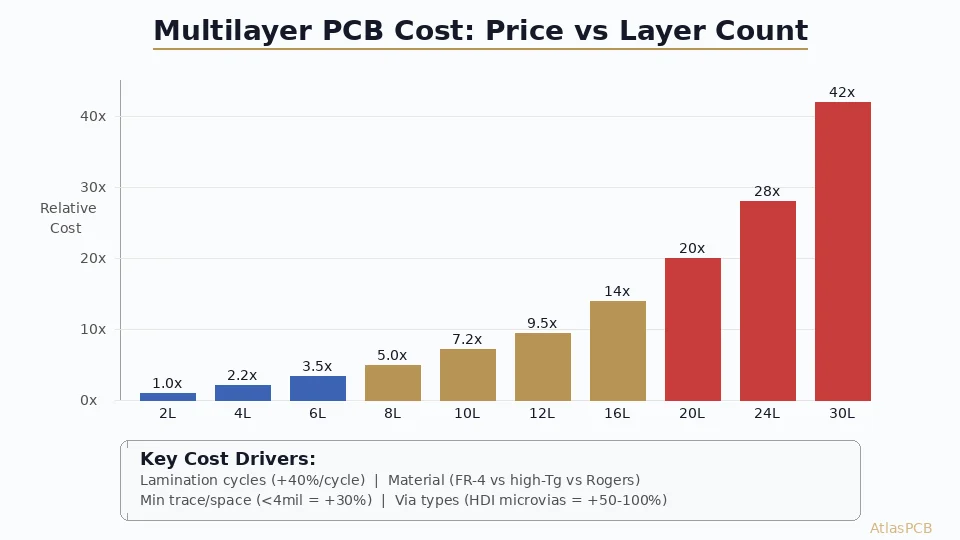
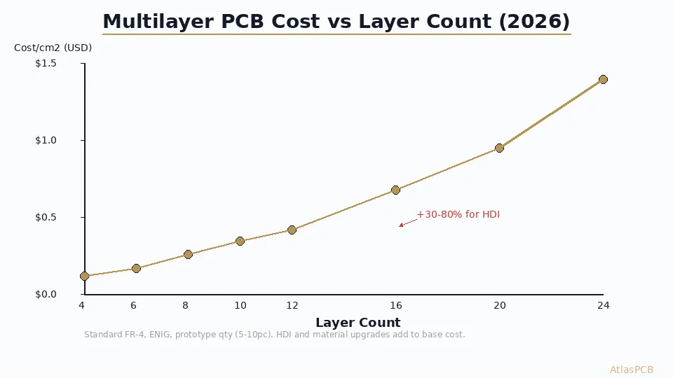
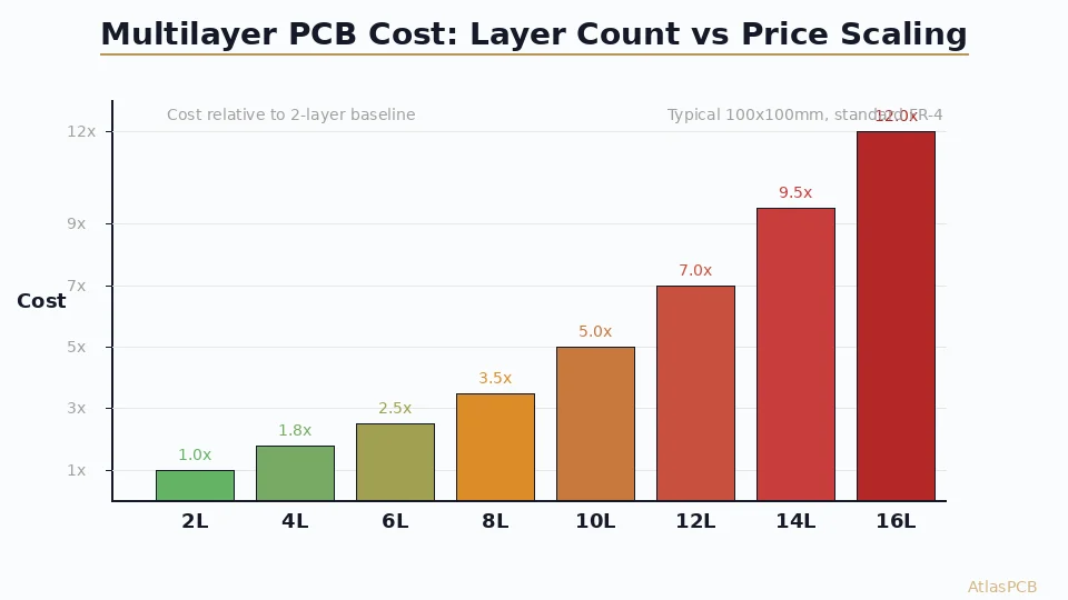
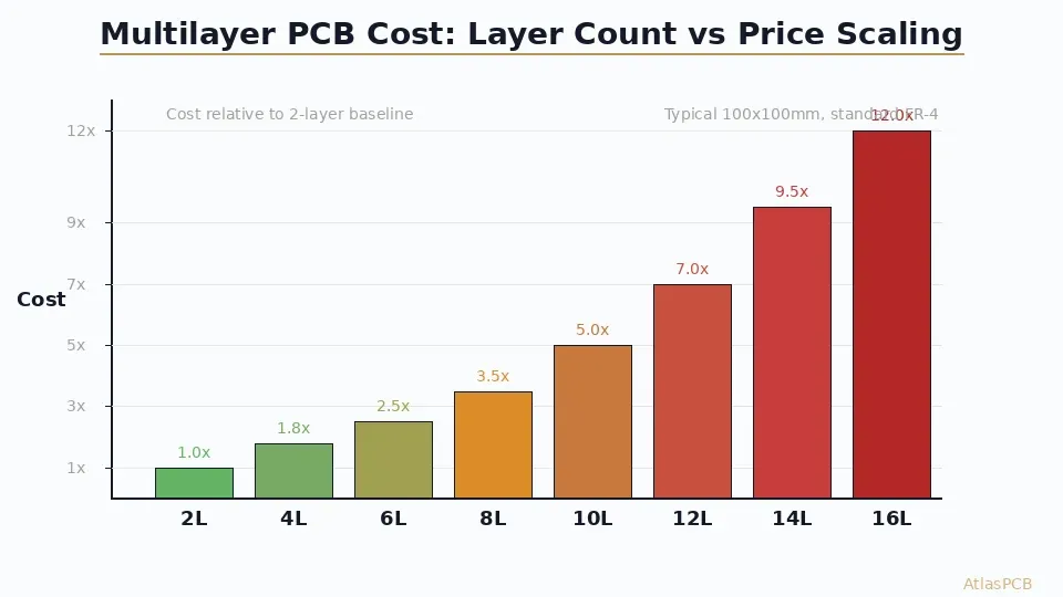
A standard 4-layer FR-4 PCB (100x100mm, 1oz copper, HASL finish) costs $8-15 per piece in quantities of 10-50 prototypes, scaling to $2-4 per piece at 1000+ units. Each additional pair of layers adds approximately 40-70% to the base cost due to extra lamination cycles, drilling passes, and yield loss. The biggest cost optimization is reducing layer count through better routing density or HDI microvias rather than simply accepting more layers.
Quick Reference: 2026 Multilayer PCB Pricing
| Layer Count | Prototype (5-10 pcs) | Mid-Volume (100 pcs) | Production (1000 pcs) | Key Cost Driver |
|---|---|---|---|---|
| 2-layer | $3-8 | $1-3 | $0.50-1.50 | Baseline |
| 4-layer | $8-15 | $3-6 | $2-4 | +1 lamination |
| 6-layer | $15-30 | $6-12 | $4-7 | +core alignment |
| 8-layer | $30-55 | $12-22 | $7-12 | Sequential lam. |
| 10-layer | $50-80 | $20-35 | $12-18 | Complex drill |
| 12-layer | $75-120 | $30-50 | $18-28 | Yield loss |
| 14-layer | $100-160 | $45-70 | $25-38 | Registration |
| 16-layer | $140-220 | $60-95 | $35-50 | Premium process |
Pricing based on: 100x100mm, standard FR-4 Tg170, 1oz copper, HASL finish, 8/8mil trace/space, standard vias. Actual pricing varies by manufacturer, material, and specific design features. Data from AtlasPCB production quotes, Q2-Q3 2026.
Why Layer Count Is Not the Only Cost Driver
Engineers often fixate on layer count as the primary cost variable, but our quoting data across 3,000+ orders this year tells a more nuanced story. Layer count establishes the baseline cost tier, but within that tier, the actual price can vary 2-3x depending on design-specific features.
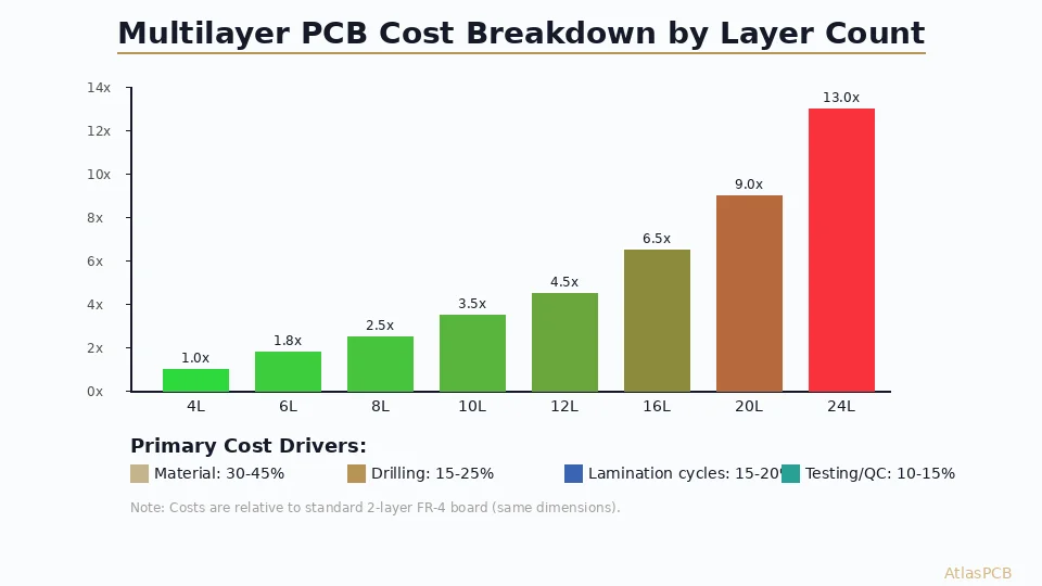
The real cost structure of a multilayer PCB breaks down into five categories, each with different weight depending on layer count:
Material cost (20-35% of total): Scales linearly with layer count because each layer pair adds a core or prepreg sheet. However, material choice matters enormously — Rogers RO4350B costs 3-5x more per layer than standard FR-4, while high-Tg FR-4 (Tg>170C) adds only 10-15% over standard.
Lamination and pressing (15-25%): This is where cost jumps non-linearly. A 4-layer board uses one press cycle. A 10-layer board with buried vias may require three sequential lamination cycles, each taking 2-3 hours of press time plus cooling. Press capacity is the most constrained resource in our factory — it directly sets throughput limits.
Drilling (10-20%): More layers means more drill hits — not just through-hole vias but potentially blind, buried, and back-drilled vias. A standard 4-layer board might have 2,000 drill hits. A 12-layer BGA-intensive design can exceed 15,000 hits with multiple drill passes at different depths.
Imaging and etching (15-20%): Each copper layer requires a separate imaging, develop, etch, strip cycle. This scales linearly with layer count but becomes more challenging as trace widths decrease on inner layers.
Testing and yield loss (10-15%): Higher layer counts have exponentially more opportunities for defects. A single open or short on any layer scraps the entire board. Our first-pass yield on 4-layer boards runs 97%+, while 12-layer boards average 92-94%, and 16-layer designs average 88-91%. That yield difference gets priced into the per-piece cost.
TRANSPARENT PRICING
Get Real-Time Multilayer PCB Pricing
Upload your Gerber files for an instant quote. Our system analyzes actual design complexity — layer count, via types, minimum features, and panel utilization — to give you accurate pricing in under 2 hours.
Get Instant Quote ›
The Features That Actually Blow Up Cost
Within any layer count tier, these design features have the largest impact on pricing. Knowing these lets you make informed tradeoffs during PCB layout:
Blind and buried vias (+30-80% over through-hole only). Every blind/buried via requires a separate drilling pass on sub-assemblies before lamination. A 6-layer board with only through-hole vias costs roughly the same as a 4-layer board with blind vias. If you can route your design with through-hole vias only, do it — the cost saving is substantial.
Via-in-pad with planarization (+20-40%). Required for fine-pitch BGAs (0.5mm and below) but adds a fill-and-planarize process step. Each via must be filled with conductive or non-conductive epoxy, then surface-planed to provide a flat pad for component soldering. This is an extra process day and a yield risk point.
Minimum trace/space below 4/4 mil (+15-30%). Standard PCB processes handle 5/5 mil (125 um) routinely. Going to 4/4 mil requires tighter imaging controls and reduces etch process window. Below 3.5/3.5 mil, you enter advanced HDI territory requiring MSAP (Modified Semi-Additive Process) — dramatically increasing cost.
Controlled impedance (+5-15%). The impedance specification itself adds modest cost (test coupon fabrication and TDR measurement). The real cost comes from tighter trace width tolerance requirements that reduce etch process window and increase inspection time.
Copper weight above 2oz (+20-50% per heavy layer). Heavy copper (2oz+) requires longer plating time, thicker resist, and careful etch control. A 4-layer board with 3oz copper on power layers costs as much as a standard 6-layer board. For high-current applications, consider copper inlay or embedded bus bars as alternatives to full-layer heavy copper.
Optimization Strategy 1: Panel Utilization
The single most impactful cost optimization for prototype and low-volume orders is panel utilization. PCBs are fabricated on standard panels (typically 18x24 inches or 457x610mm working area). Your board’s dimensions and the manufacturer’s panelization determine how many boards fit per panel.
Consider a 50x80mm board on a standard 457x610mm panel. With standard routing gaps (2mm) and panel borders (10mm), you can fit approximately 42 boards per panel. But a 55x85mm board — just 5mm larger in each dimension — drops to 35 boards per panel. That is a 17% reduction in panel utilization, which directly translates to 17% higher per-piece cost at volume.
Practical optimization approaches:
Design to panel-friendly dimensions. Ask your manufacturer for their standard panel working area and design your board outline to maximize fit. Even 1-2mm of dimensional flexibility can add an extra row or column of boards per panel.
Optimize quantity to fill panels. If 42 boards fit per panel, ordering 42 (or 84, or 126) gives you the best per-piece price. Ordering 50 means you pay for 2 panels but only use 92% of the second panel’s capacity. Many manufacturers price per panel anyway — ask for the quantity that gives you “free” extra boards.
Consider mixed panelization. If you have multiple small PCBs in the same design (e.g., main board + daughter board + test fixture), the manufacturer may be able to panelize them together, sharing setup and material costs across all designs.
Based on production data from our quoting system, optimizing panelization typically saves 15-25% on orders under 500 pieces. The saving diminishes at high volume where panel utilization is already maximized.
Optimization Strategy 2: Via Architecture Decisions
Your via strategy has a disproportionate impact on multilayer PCB cost because it determines how many sequential lamination cycles are needed. Here is the cost hierarchy:
Through-hole vias only (baseline cost): Single drill pass after final lamination. Available on all manufacturers. Maximum routing flexibility sacrifice (vias consume space on all layers). Best for: designs where routing density is not critical and board real estate is available.
Blind vias only — 1+N+1 buildup (+30-50%): One additional sub-assembly step. Microvias from L1 to L2 and LN to LN-1. Enables BGA breakout without through-hole via fields. Best for: fine-pitch BGAs (0.5-0.8mm) on boards up to 8 layers where routing density is moderate.
Blind + buried vias (+50-80%): Multiple sub-assembly steps. Buried vias (e.g., L2-L5) formed on inner sub-assemblies before final lamination. Significantly increases routing density on inner layers. Best for: high-density 8-12 layer designs with multiple BGA devices.
Stacked microvias — 2+N+2 or 3+N+3 (+80-150%): Multiple sequential buildup cycles. Enables via stacking for ultra-high-density routing. Requires careful reliability qualification (IPC-2315 considerations). Best for: mobile device boards, SiP modules, and designs with sub-0.4mm pitch BGAs.
In our experience, the decision between through-hole and 1+N+1 HDI is often the biggest leverage point. If your 8-layer through-hole design is driven purely by BGA breakout routing, switching to a 6-layer 1+N+1 HDI design may cost the same while reducing board area by 20-30%.
COST OPTIMIZATION
Not Sure About the Most Cost-Effective Layer Count?
Send us your netlist and component placement. Our engineering team can recommend whether HDI microvias, additional layers, or a larger board area gives you the best price-performance ratio for your specific design.
Compare Options ›Optimization Strategy 3: Material and Finish Selection
Material and surface finish choices compound with layer count. A 12-layer board with ENIG finish and controlled impedance on Rogers layers can cost 4-5x the same layer count in standard FR-4 with HASL. Here are the cost-effective defaults and when to deviate:
Default choices (lowest cost at acceptable quality):
- FR-4 Tg170 (standard mid-range, adequate for lead-free assembly)
- 1oz copper (sufficient for most signal and moderate power)
- HASL lead-free (cheapest finish, adequate for components with pitch >0.8mm)
- Standard board thickness 1.6mm (optimized press programs, no special handling)
When to upgrade (justified cost increases):
- ENIG: Required for BGA pitch below 0.8mm, gold wire bonding, or corrosion-sensitive environments. Adds $0.50-1.50/piece prototype, $0.15-0.30/piece at volume.
- 2oz copper: Required when current density exceeds 1A per trace at your width, or for power planes feeding >10A total load.
- High-Tg (Tg>180): Required for lead-free assembly with multiple reflow cycles (double-sided SMT) or high-reliability applications.
- Rogers: Required above 3 GHz for RF layers (covered in our FR-4 vs Rogers guide).
Common over-specifications we see (cost added with no benefit):
- ENIG on a board with only through-hole components and 1.27mm pitch connectors — HASL works fine
- 2oz copper on signal-only layers carrying milliamp-level digital signals — 0.5oz saves cost
- Immersion silver “for better solderability” on a prototype that ships within 30 days — HASL solders perfectly with fresh boards
- Rogers on a 900 MHz LoRa radio — FR-4 works at 900 MHz with generous loss margin
Real Cost Example: 8-Layer BGA Board
To illustrate how these factors compound, here is a real pricing breakdown from a production quote we processed in June 2026. The customer’s design: 8-layer, 80x60mm, two 0.65mm-pitch BGAs, DDR4 memory, USB 3.0, controlled impedance.
| Cost Component | Percentage | Absolute (per piece @ 200 qty) |
|---|---|---|
| Material (FR-4 Tg170, 8 layers) | 28% | $4.20 |
| Lamination (2 press cycles) | 18% | $2.70 |
| Drilling (6,200 holes, 2 drill passes) | 15% | $2.25 |
| Imaging and etch (8 layers) | 14% | $2.10 |
| Via-in-pad fill + planarize | 8% | $1.20 |
| ENIG surface finish | 5% | $0.75 |
| Impedance coupons + TDR test | 4% | $0.60 |
| AOI + electrical test + yield | 8% | $1.20 |
| Total per piece | 100% | $15.00 |
At prototype quantity (10 pieces), the same board costs approximately $42/piece — the per-panel fixed costs are amortized over fewer boards.
VOLUME PRICING
See How Quantity Breaks Affect Your Design
Upload your Gerbers and select multiple quantities. Our quoting system shows pricing at 10, 50, 100, 500, and 1000+ pieces so you can plan production scaling with real cost data.
Get Volume Pricing ›When Higher Layer Count Saves Money Overall
Counterintuitively, adding layers sometimes reduces total product cost. The decision depends on whether board area or layer count is your binding constraint:
Scenario: Dense IoT module with BLE + sensors. An engineer routes the design on a 6-layer board at 45x55mm. The board cost is $10/piece at 500 qty. A redesign on 8 layers reduces the board to 30x35mm. The 8-layer board costs $12/piece, but the 40% area reduction saves $2/piece on the enclosure tooling, $0.50/piece on shipping weight, and enables a smaller product form factor that commands premium pricing.
Scenario: Server board with 4 DDR5 channels. The initial 12-layer design uses extensive routing on inner layers with through-hole vias. Yield runs at 89% due to dense inner-layer routing. A 14-layer redesign with wider trace spacing on each layer improves yield to 95%. The 2 extra layers add $3/piece, but the 6% yield improvement saves $4.50/piece in scrapped panels. Net savings: $1.50/piece.
The principle: evaluate total landed cost (PCB + assembly + enclosure + yield + logistics) rather than bare board cost in isolation. Our engineering team routinely helps customers model these tradeoffs during the design phase, before committing to a layer count.
Summary: Getting the Best Value from Multilayer PCBs
The most cost-effective multilayer PCB is not the cheapest per-board — it is the one that closes your design requirements at the lowest total product cost with acceptable risk. Focus your optimization effort on:
- Panel utilization (order quantities that fill panels)
- Via architecture (through-hole vs. HDI — biggest binary cost decision)
- Material selection (do not over-specify materials or finish)
- Layer count optimization (sometimes more layers = less total cost)
- Design for manufacturing (stay within standard process parameters)
ATLASPCB
Ready to Get Accurate Multilayer Pricing?
Upload your design files and get a detailed quote with cost breakdown by layer count, material, and process features. We include optimization suggestions that can save 15-30% without design changes.
Get Detailed Quote ›
Reviewed by AtlasPCB Engineering Team — 15+ years in advanced PCB fabrication for RF, HDI, and rigid-flex applications.
Related Reading:
About AtlasPCB — We specialize in complex PCB manufacturing for HDI, RF, and high-reliability applications. Explore our HDI PCB manufacturing capabilities, multilayer PCB fabrication up to 30 layers, or get an PCB prototype manufacturing from 1 piece . Every order includes free engineering review. Get your quote.
Reviewed by AtlasPCB Engineering Team — IPC-certified manufacturing specialists with 15+ years of production experience in HDI, RF, and high-reliability PCB fabrication. Content based on factory floor data and real customer design reviews.
Frequently Asked Questions
How much does a 4-layer PCB prototype cost?
Why does cost jump significantly at 8+ layers?
Is HDI more expensive than adding layers?
What is the cost difference between HASL and ENIG finish?
How can I reduce multilayer PCB cost without compromising performance?
- multilayer PCB cost
- PCB pricing
- HDI PCB cost
- PCB prototype cost
- PCB manufacturer pricing