· Sophia Reyes · Engineering · 8 min read
PCB Stackup Design Guide
A practical guide to PCB stackup design covering signal/ground layer assignment, impedance target planning, prepreg and core selection, and manufacturing DFM constraints. Focused on getting your stackup right before you order.
Quick Answer
A well-designed PCB stackup assigns signal layers adjacent to unbroken ground planes for impedance reference, uses symmetric construction to prevent warpage, specifies exact prepreg/core thicknesses to hit impedance targets, and follows manufacturer DFM constraints for minimum dielectric spacing and copper balance.
The 30-Second Stackup Decision
| Layer Count | Recommended Assignment | Best For |
|---|---|---|
| 4-layer | SIG-GND-PWR-SIG | Simple mixed-signal, cost-optimized |
| 6-layer | SIG-GND-SIG-PWR-GND-SIG | USB3/PCIe Gen3, moderate density |
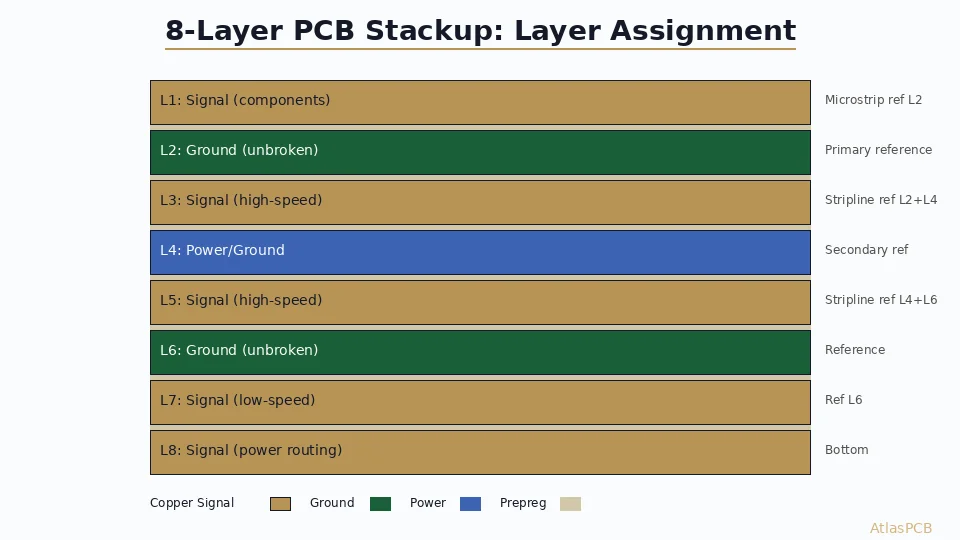
| 8-layer | SIG-GND-SIG-GND-PWR-SIG-GND-SIG | DDR4/5, PCIe Gen4+, RF |
| 10-layer | SIG-GND-SIG-GND-PWR-GND-SIG-GND-SIG-SIG | High-density BGA breakout |
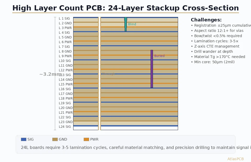
| 12-16 layer | Follow 60/40 rule: 60% reference planes | Server, networking, FPGA |
The single most important principle: every high-speed signal layer must have an adjacent, unbroken reference plane. Everything else is secondary.
Layer Assignment: The Foundation of Signal Integrity
The assignment of signal and reference plane layers determines your board’s impedance characteristics, crosstalk performance, and EMI behavior before you route a single trace. Getting this wrong is the single most common cause of signal integrity failures that we catch during DFM review.
For a standard 4-layer board, the optimal assignment is straightforward: signal on L1, ground plane on L2, power plane on L3, signal on L4. This gives both outer signal layers an adjacent ground reference at a controlled dielectric distance. The L2 ground plane serves as the impedance reference for L1 traces, while L3 power plane (with adequate decoupling) serves as the reference for L4.
The common mistake engineers make is placing signals on L2 and L3 (the inner layers) with ground/power on the outside. While this seems logical for EMI containment, it actually creates worse signal integrity because the inner signal layers are sandwiched between two planes at different potentials, creating unpredictable reference transitions when traces cross plane splits.
For 6-layer and above, the principle scales: maintain a reference plane adjacent to every signal layer. In our production data, boards that follow this rule achieve first-pass impedance compliance at rates above 96%, compared to 78% for boards with “creative” stackup assignments that violate the adjacency principle.
PCB STACKUP DESIGN SUPPORT
Not Sure About Your Stackup?
Upload your design files and our process engineers will simulate your stackup against actual material inventory, confirm impedance targets are achievable, and suggest optimizations.
Request Stackup Review ›
Prepreg and Core Selection: The Numbers That Actually Matter
A stackup drawing is only as good as the materials specified in it. Many engineers specify “FR-4” without realizing that this is a material class, not a single product — and different prepreg styles within the same class have dramatically different thicknesses after lamination.
Common Prepreg Styles and Pressed Thicknesses (FR-4, Tg 170)
| Style | Glass Weave | Nominal Thickness | Pressed Thickness (1 ply) | Resin Content |
|---|---|---|---|---|
| 1080 | Thin, tight weave | 0.076mm (3.0mil) | 0.066-0.073mm | 65% |
| 2116 | Medium weave | 0.120mm (4.7mil) | 0.105-0.115mm | 52% |
| 7628 | Thick, open weave | 0.185mm (7.3mil) | 0.175-0.185mm | 42% |
The pressed thickness (after lamination) is what determines your impedance. This is different from the nominal thickness that appears on datasheets. When a manufacturer receives your stackup specifying “5mil dielectric,” they need to figure out which combination of prepreg plies achieves that target — and available options are not infinite.
A single ply of 1080 gives you approximately 2.7mil pressed thickness. Two plies of 1080 give 5.4-5.8mil. One ply of 2116 gives about 4.2mil. These are the building blocks, and your impedance target must be achievable with some combination of these standard materials.
In our experience, approximately 25% of first-time stackup submissions specify dielectric thicknesses that do not correspond to any available prepreg combination. For example, requesting 3.5mil dielectric spacing is problematic — it falls between 1x1080 (2.7mil) and 1x2116 (4.2mil), with no standard single-ply option available.
Practical Impedance Planning Process:
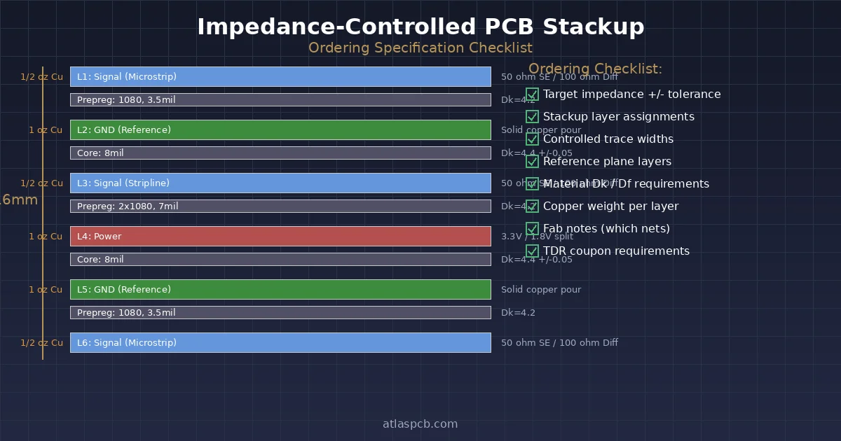
Start with your impedance target (typically 50-ohm single-ended, 100-ohm differential), work backward to the required trace width and dielectric thickness using a 2D field solver, then verify that the calculated dielectric thickness is achievable with available prepreg combinations. If it is not, adjust trace width to accommodate the nearest available dielectric option.
Impedance Planning: Getting to +/-5% on the First Build
Achieving tight impedance tolerance is not about specifying a number on a drawing — it is about designing a stackup where the manufacturing process naturally produces the correct impedance. This means understanding what the manufacturer can control and what varies.
Controllable parameters (tight tolerance possible):
- Trace width: +/-0.5mil with LDI exposure
- Copper thickness: +/-3um with precise plating
- Prepreg ply count: exact (digital — either it is there or not)
Semi-controllable parameters (moderate variation):
- Pressed dielectric thickness: +/-8% across a panel
- Resin fill around traces: depends on copper density
- Dk value: +/-3% between lots
The practical implication is that your impedance target should have design margin built in. If you need 50 ohms +/-5% (47.5-52.5 ohms), design your stackup to nominally produce 50.0 ohms at the center of all tolerance windows. Do not design to exactly 47.5 ohms hoping everything lands on the low side.
For differential pairs, the coupling between traces adds another variable. The gap between differential traces must be controlled to the same precision as trace width, which means your differential impedance tolerance is inherently slightly wider than single-ended. Design for 100-ohm differential with minimum 4mil gap to give the process adequate margin.
IMPEDANCE-CONTROLLED MANUFACTURING
TDR-Verified Impedance on Every Panel
We run impedance simulation before production and verify with TDR coupon testing on every production panel. Typical first-pass yield: 96%+ for +/-5% tolerance.
Common Stackup DFM Violations We Catch
Based on reviews we have performed in the past six months, these are the most frequent stackup-related DFM issues that cause fabrication problems or impedance failures:
1. Copper weight imbalance causing warpage
A 10-layer board with 2oz copper on layers 1-5 and 0.5oz on layers 6-10 will bow like a banana after lamination. The thermal expansion coefficient difference between heavy copper and light copper layers creates internal stress. Our DFM review flags any design where copper weight differs by more than 1oz between the top and bottom halves.
2. Insufficient dielectric for voltage withstand
IPC-2221B specifies minimum conductor spacing based on voltage. A common error is placing a 48V power plane only 3mil away from an adjacent signal layer — below the 5mil minimum for 50V DC per the standard. This is rarely caught by EDA design rule checks because most DRCs do not cross-reference voltage assignments against stackup spacing.
3. Asymmetric plane splits creating impedance discontinuities
When a ground plane is split for isolation purposes (analog/digital separation, for example), traces crossing the split lose their impedance reference and radiate EMI. We recommend adding a row of stitching vias along the split boundary and routing sensitive traces at least 20mil away from any plane edge.
4. Via aspect ratio exceeding plating capability
A 2.4mm thick board with 0.15mm drill holes creates a 16:1 aspect ratio — at the absolute limit of reliable copper plating. The via barrel may be thin at the center, creating a reliability risk. If your stackup produces a total thickness above 2.0mm, either increase drill diameter or plan for sequential lamination with shorter via spans.
DFM REVIEW
Catch Stackup Issues Before Production
Our process engineers review layer assignments, dielectric specifications, and copper balance against actual fabrication constraints. We flag issues that EDA tools miss.
Submit for DFM Review ›Stackup Templates: Starting Points for Common Applications
Rather than designing from scratch, start with a proven stackup template and modify only what your design specifically requires. Here are field-proven configurations from our production database:
4-Layer Standard (Cost-Optimized, General Digital)
- L1: Signal (1oz) — microstrip
- Prepreg: 2x1080 (0.15mm)
- L2: GND (1oz) — full plane
- Core: 1.0mm
- L3: PWR (1oz) — full plane
- Prepreg: 2x1080 (0.15mm)
- L4: Signal (1oz) — microstrip
- Total: 1.6mm | 50-ohm SE: 5.2mil trace | 100-ohm diff: 4.5/5.0mil trace/gap
8-Layer High-Speed Digital (DDR4/5, PCIe Gen4)
- L1: Signal (1oz)
- PP: 1x2116 (0.105mm)
- L2: GND (0.5oz)
- Core: 0.2mm
- L3: Signal (1oz)
- PP: 2x1080 (0.15mm)
- L4: GND (0.5oz)
- Core: 0.4mm
- L5: PWR (0.5oz)
- PP: 2x1080 (0.15mm)
- L6: Signal (1oz)
- Core: 0.2mm
- L7: GND (0.5oz)
- PP: 1x2116 (0.105mm)
- L8: Signal (1oz)
- Total: 1.6mm | Stripline 50-ohm: 3.8mil trace
These templates are production-proven — we have fabricated hundreds of panels with these exact configurations and have characterized the actual impedance achieved. Starting from a known-good stackup eliminates the most common source of iteration in new designs.
ATLASPCB
Need a Production-Proven Stackup for Your Design?
Upload your design files and we will recommend an optimized stackup from our production-characterized library. Includes impedance simulation against actual material inventory.
Get Stackup Recommendation ›
Reviewed by AtlasPCB Engineering Team — 15+ years in advanced PCB fabrication for RF, HDI, and rigid-flex applications.
Related Reading:
About AtlasPCB — We specialize in complex PCB manufacturing for HDI, RF, and high-reliability applications. Explore our impedance-controlled PCB manufacturing, or get an free engineering DFM review . Every order includes free engineering review. Get your quote.
Reviewed by AtlasPCB Engineering Team — IPC-certified manufacturing specialists with 15+ years of production experience in HDI, RF, and high-reliability PCB fabrication. Content based on factory floor data and real customer design reviews.
Frequently Asked Questions
How do I choose between microstrip and stripline for impedance-controlled traces?
What prepreg thickness should I use for 50-ohm impedance?
Why does my manufacturer reject my stackup drawing?
How many ground planes do I need in a 6-layer board?
Does stackup symmetry really matter?
- PCB stackup design
- impedance control
- DFM
- multilayer PCB
- PCB design guide