· AtlasPCB Engineering · Engineering · 9 min read
HDI PCB Manufacturer Pricing: Understanding the Cost Gap Between 1+N+1 and 2+N+2 Microvia Builds
A transparent breakdown of HDI PCB pricing across microvia technology tiers. Explains why 2+N+2 costs 80-120% more than 1+N+1, where the cost actually comes from, and 5 design strategies that reduce your HDI quote by 25-35% without compromising routing density or signal performance.
Quick Answer
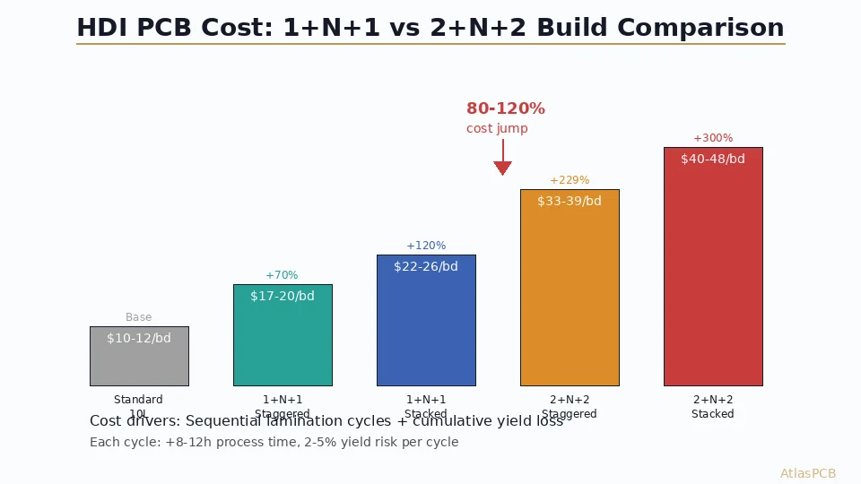
The cost jump from 1+N+1 HDI to 2+N+2 HDI is 80-120% — not the 2x you might expect from doubling buildup layers. The primary cost driver is sequential lamination: each additional lamination cycle adds a full press-etch-drill sequence that doubles process time and yield risk. A 10-layer 2+N+2 board costs $28-45/board at 200 pieces, versus $14-22/board for an equivalent 10-layer 1+N+1. Design strategies like staggered microvias (instead of stacked), selective HDI (one side only), and increasing core layer count can reduce 2+N+2 pricing by 25-35%.
Quick Cost Reference: HDI PCB Pricing by Build Type
| HDI Configuration | Typical Layers | Cost per Board (200 pcs, 50x50mm) | vs Standard Through-Hole |
|---|---|---|---|
| Standard (no HDI) | 10L | $8-12 | Baseline |
| 1+N+1 (staggered) | 10L | $14-18 | +60-80% |
| 1+N+1 (stacked) | 10L | $18-24 | +100-130% |
| 2+N+2 (staggered) | 10L | $28-38 | +180-250% |
| 2+N+2 (stacked) | 10L | $35-45 | +230-310% |
| 3+N+3 (any-layer) | 12L | $55-80 | +400-550% |
These are production pricing ranges from our facility at 200-piece volume for 50x50mm boards with standard FR-4 material. Your actual quote depends on board size, copper weight, surface finish, and specific design features.
Where HDI Cost Actually Comes From
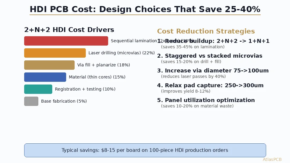
Engineers often assume HDI pricing is primarily driven by the laser drilling step — after all, it requires expensive UV or CO2 laser systems that cost $500K-1.5M per machine. In reality, laser drilling accounts for only 15-20% of the HDI price premium. The dominant cost drivers are sequential lamination and the yield mathematics of multi-cycle processing.
A standard through-hole PCB — regardless of layer count — goes through exactly one lamination press cycle. All layers are aligned, pressed together, and then drilled and plated in a single continuous flow. The entire manufacturing sequence from innerlayer imaging to final routing takes 5-7 working days for a 10-layer board.
A 2+N+2 HDI board goes through a fundamentally different process architecture. First, the core layers (the “N” in the middle) are fabricated as a conventional multilayer board. Then, buildup layers are added sequentially — one layer at a time on each side, with a complete press-drill-plate cycle between each addition. Each cycle must be completed and inspected before the next can begin, creating a serial process dependency that cannot be parallelized.
In our facility, each sequential lamination cycle adds approximately 8-12 hours of process time (including press cure, laser drill, microvia plating, and inspection). A 2+N+2 board requires 4 cycles total — meaning the HDI portion alone takes 32-48 hours of sequential processing that cannot be batched with other jobs the way standard multilayer panels can.
HDI MANUFACTURING
Get a Transparent HDI Quote With Cost Breakdown
We itemize NRE, sequential lamination, microvia processing, and testing costs separately — so you know exactly what drives your price.
Upload HDI Design ›
Yield Mathematics: The Hidden Cost Multiplier
The second major cost driver in HDI manufacturing is cumulative yield loss. Each sequential lamination cycle introduces process risk — misregistration between buildup layers and the core, laser drill quality variation, microvia plating voids, and lamination defects. In a well-controlled facility, individual cycle yield for 1+N+1 HDI runs 95-98%. But these yields multiply across multiple cycles.
Here is what that multiplication looks like in practice:
| Build Type | Lamination Cycles | Per-Cycle Yield | Cumulative Yield | Effective Cost Multiplier |
|---|---|---|---|---|
| 1+N+1 | 2 | 97% | 94.1% | 1.06x |
| 2+N+2 | 4 | 97% | 88.5% | 1.13x |
| 3+N+3 | 6 | 97% | 83.3% | 1.20x |
| 2+N+2 (stacked) | 4 | 95% | 81.5% | 1.23x |
| Any-layer (stacked, 4 cycles) | 4 | 93% | 74.8% | 1.34x |
The yield difference between staggered and stacked microvias is significant. Stacked vias require copper filling of the lower via before the upper via is drilled on top of it — adding a copper fill and planarization step that has its own yield risk. Staggered vias offset each level’s landing pad, eliminating the fill requirement and improving per-cycle yield by 2-3 percentage points.
At 200-piece production volume, a 1.13x yield multiplier adds $2-4 per board in waste allocation. At 1.34x (any-layer with stacked vias), it adds $6-10 per board. These costs are invisible in the per-unit quote but represent real material and machine time consumed by rejected panels that never ship.
Our facility achieves slightly better-than-industry yields because we operate dedicated HDI lines with registration accuracy below +/-25um (compared to +/-50um typical). This registration precision directly translates to fewer misalignment rejects on 2+N+2 and higher builds. We pass this yield advantage to customers as lower pricing rather than higher margins — which is why dedicated HDI manufacturers consistently quote lower than general-purpose PCB shops for complex HDI designs.
Five Design Changes That Cut Your HDI Quote by 25-35%
Based on our analysis of 1200+ HDI quotes over the past year, here are the design optimizations that deliver the largest cost reductions without compromising electrical performance:
1. Staggered microvias instead of stacked (saves 15-20%).
Stacked microvias require copper filling the lower via level before drilling the upper level on top. This adds a copper electroplating fill step ($0.80-1.50/board), a surface planarization step ($0.30-0.50/board), and reduces yield by 2-3%. Staggered microvias offset each level’s landing pad by at least 100um, allowing standard plating and eliminating the fill requirement entirely. Unless your BGA pitch absolutely requires stacked vias for breakout (0.4mm pitch and below), staggered vias provide equivalent routing density at significantly lower cost.
2. Apply HDI on one side only — 1+N+0 or 2+N+0 (saves 30-40%).
If your fine-pitch components are exclusively on one board side (common for single-sided BGA designs), you only need buildup layers on that side. A 1+N+0 build cuts sequential lamination cycles in half compared to 1+N+1, and eliminates all HDI processing on the bottom side. We see this opportunity in approximately 40% of HDI designs we review — engineers default to symmetric buildup without analyzing whether the bottom side actually needs microvias.
3. Increase core layer count to reduce buildup complexity (saves 10-25%).
Sometimes a 2+4+2 design (two buildup layers on each side of a 4-layer core) can be refactored into a 1+6+1 design (one buildup layer on each side of a 6-layer core) by adding two more conventionally-drilled inner layers. The additional core layers cost roughly $2-3/board, while eliminating one sequential lamination cycle saves $8-12/board. The tradeoff: you need slightly more routing space on conventional layers, and your through-vias may require backdrilling for high-speed signals.
4. Avoid via-in-pad where alternative fan-out exists (saves $0.50-1.50/board).
Via-in-pad (VIPPO) requires copper filling and planarization — both adding process steps and yield risk. For BGAs at 0.8mm pitch and above, dog-bone fan-out with standard vias (placed outside the pad) provides adequate routing escape without via-in-pad. Even at 0.65mm pitch, careful routing can often avoid VIPPO on outer-ring pads, requiring it only for inner-row balls. Every via-in-pad avoided reduces your cost incrementally.
5. Keep microvia aspect ratio below 0.8:1 (avoids premium processing).
Standard CO2 laser drill parameters work reliably for microvia depths up to 80% of the via diameter. For our standard 100um (4mil) laser via, this means the dielectric buildup thickness should stay below 80um. Deeper microvias require slower laser parameters, multiple pulse sequences, or UV laser (5x more expensive per hole). Design your buildup layer thickness to keep aspect ratio in the safe zone: 60-75um prepreg for 100um vias, or use 125um (5mil) vias if you need thicker dielectric.
DESIGN OPTIMIZATION
Let Us Optimize Your HDI Design for Cost
Send your current design — we identify opportunities to reduce build complexity and quote both the original and optimized version side by side.
When Budget HDI Services Fall Short
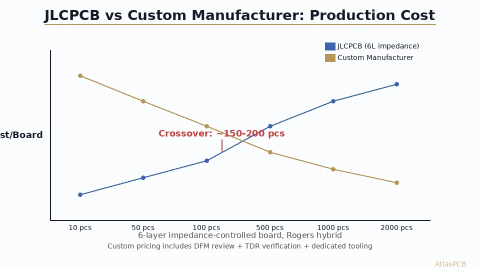
JLCPCB and similar automated ordering platforms offer 1+N+1 HDI at competitive prices for prototypes and small production runs. Their pricing works because they pool HDI panels from multiple customers, optimize laser drill utilization, and standardize their sequential lamination process. For 1+N+1 staggered microvias on standard FR-4, budget services deliver perfectly adequate quality.
The limitations appear with 2+N+2 builds and above. Budget services typically route these orders to partner factories with premium pricing (passing through 15-25% margin), provide minimal DFM review (no stackup optimization, no yield risk assessment), and offer limited documentation (no cross-section reports, no registration measurement data).
For production HDI at 200+ pieces, the value proposition of a dedicated HDI manufacturer includes engineering review that identifies cost reduction opportunities (often reducing the quote by 15-25% through design optimization), yield guarantees backed by process data, and documentation that proves your boards meet specification before they ship.
In our experience, 30-40% of 2+N+2 HDI designs we receive for quoting can be redesigned as 1+N+1 with one additional core layer — immediately cutting 40-50% from the price. Budget services have no incentive to identify this opportunity because they price what you submit without engineering analysis.
Getting an Accurate HDI Quote: What to Include
To receive a realistic HDI quote (not a lowball that escalates after design review), provide your manufacturer with:
- Full Gerber package including drill files that clearly distinguish laser vias from mechanical vias
- Stackup specification showing which layers are buildup and which are core
- Via structure definition: stacked vs staggered, via-in-pad locations, fill requirements
- Impedance requirements per signal layer (affects prepreg selection and thickness constraints)
- Production volume and delivery timeline (HDI lead time is 12-18 working days typically)
Missing any of these items results in either an overly conservative quote (manufacturer assumes worst case) or an inaccurate quote that requires revision after engineering review — wasting time for both sides.
ATLASPCB
Ready to Quote Your HDI Design?
Upload your Gerbers for a detailed HDI quote with cost breakdown. We identify optimization opportunities and quote both original and optimized options.
Get HDI Quote ›
Reviewed by AtlasPCB Engineering Team — 15+ years in advanced PCB fabrication for RF, HDI, and rigid-flex applications.
Related Reading:
About AtlasPCB — We specialize in complex PCB manufacturing for HDI, RF, and high-reliability applications. Explore our HDI PCB manufacturing capabilities, impedance-controlled PCB manufacturing, or get an free engineering DFM review . Every order includes free engineering review. Get your quote.
Reviewed by AtlasPCB Engineering Team — IPC-certified manufacturing specialists with 15+ years of production experience in HDI, RF, and high-reliability PCB fabrication. Content based on factory floor data and real customer design reviews.
Frequently Asked Questions
Why does 2+N+2 HDI cost so much more than 1+N+1?
Can I get 2+N+2 HDI from JLCPCB or similar budget services?
What is the minimum order quantity where HDI pricing becomes reasonable?
How can I reduce my HDI PCB quote without changing my BGA?
What should an HDI manufacturer quote include that budget services skip?
- HDI PCB manufacturer
- multilayer PCB cost
- impedance controlled PCB manufacturer
- PCB DFM check
- JLCPCB vs custom PCB manufacturer