· AtlasPCB Engineering · Engineering · 9 min read
Multilayer PCB Cost 2026: Real Pricing from 4-Layer to 20-Layer Boards
Transparent multilayer PCB pricing breakdown for 2026 covering layer count premiums, material costs, HDI adders, and practical strategies to reduce cost without sacrificing performance.
Quick Answer
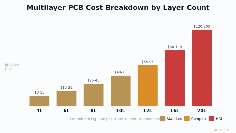
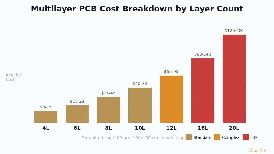
Multilayer PCB cost in 2026 scales approximately 1.4-1.6x per additional pair of layers: a standard 4-layer 100x100mm board runs $8-15/unit at 100 pieces, while 8-layer costs $25-45, 12-layer reaches $55-95, and 20-layer boards hit $120-200/unit — with material choice, via technology, and copper weight as the primary cost multipliers beyond layer count.
Quick Reference: 2026 Multilayer PCB Pricing
| Layer Count | Price/Unit (100 pcs, 100x100mm) | Lead Time | Primary Cost Driver |
|---|---|---|---|
| 4-layer | $8-15 | 5-7 days | Base cost |
| 6-layer | $15-28 | 7-10 days | +1 lamination cycle |
| 8-layer | $25-45 | 8-12 days | Material + registration |
| 10-layer | $40-70 | 10-14 days | Sequential may be needed |
| 12-layer | $55-95 | 12-16 days | Via aspect ratio limits |
| 16-layer | $80-140 | 14-18 days | Sequential lamination typical |
| 20-layer | $120-200 | 16-22 days | Complex via structures |
These ranges assume standard FR-4 (Tg 150-170C), 1oz outer / 0.5oz inner copper, ENIG finish, and no HDI features. Actual pricing varies by manufacturer, material grade, and specific design complexity. All prices are from Chinese manufacturers at factory-direct pricing — domestic US/EU pricing runs 2-3x higher.
The Layer Count Premium: Why Each Pair Costs More Than the Last
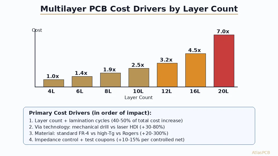
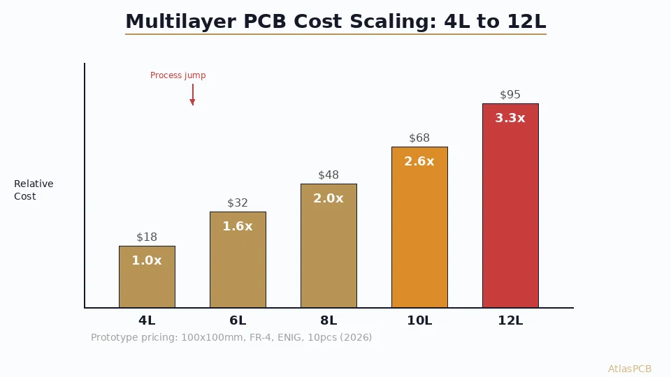
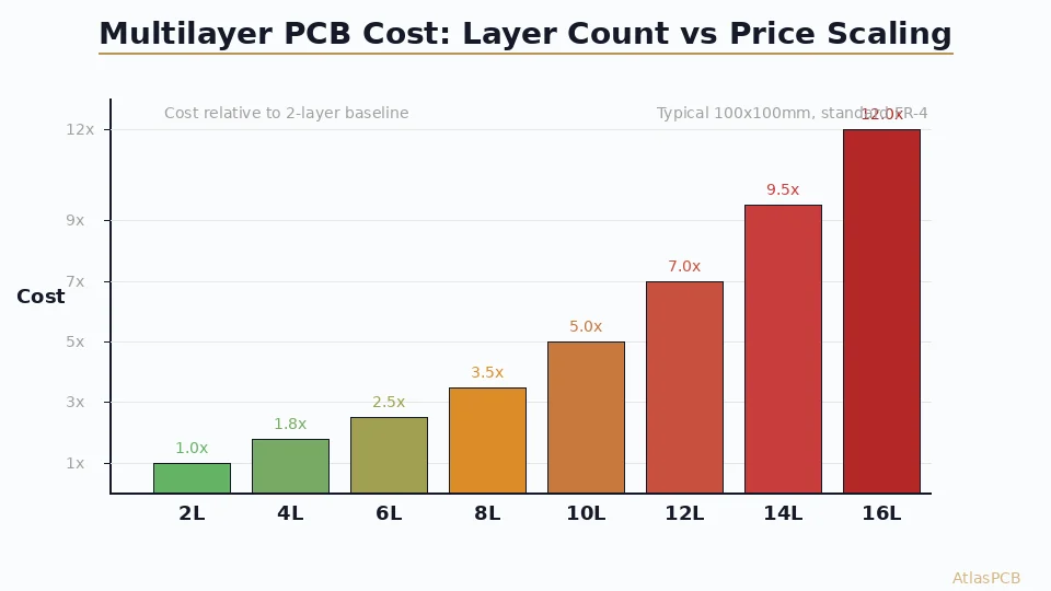
Multilayer PCB pricing does not scale linearly with layer count — it accelerates. A 12-layer board does not cost 3x a 4-layer board; it typically costs 5-7x. Understanding why helps you make informed design trade-offs between routing density and manufacturing cost.
The fundamental cost driver is lamination cycles. A 4-layer board requires a single lamination press: two cores bonded with prepreg, drilled, plated, done. A 6-layer board adds one more lamination. An 8-layer adds two. But at 10-12 layers, the via aspect ratio (board thickness divided by drill diameter) often exceeds the 10:1 limit for reliable single-pass mechanical drilling. This forces either sequential lamination (multiple press cycles with interleaved drilling) or back-drilling — both adding significant process time and cost.
In our facility, the cost breakdown for a typical 10-layer board at 100x100mm looks approximately like this: raw materials (FR-4 laminate, copper foil, prepreg) account for 25-30% of the total cost. Drilling represents 15-20% — a 10-layer board with 3000 holes requires multiple drill bit changes and precise depth control. Lamination and pressing account for another 15-20%. The remainder covers imaging, plating, etching, solder mask, surface finish, testing, and handling. As layer count increases, material and lamination costs grow proportionally, while imaging and drilling grow super-linearly due to increasing complexity.
MULTILAYER PCB PRICING
Get Exact Pricing for Your Layer Count
Upload your Gerbers or specify your stackup requirements. Pricing typically returned within 4 hours for standard multilayer designs.
Get Instant Quote ›
Material Cost: The Hidden Multiplier
Material selection impacts multilayer PCB cost far more than most engineers realize. Standard FR-4 (Shengyi S1000-2 or equivalent) at Tg 150C is the baseline. Moving to high-Tg material (Tg 170C, like Shengyi S1000-2M) adds 15-20% to material cost. Specifying halogen-free construction (required for some automotive and consumer electronics applications) adds another 10-15%.
The real cost jumps happen with specialty materials. Rogers 4350B on even two layers of an 8-layer stackup doubles the material cost. Panasonic Megtron 6 for 112G SerDes adds 80-120% to laminate cost. Isola I-Speed or similar ultra-low-loss laminates for 56G PAM4 sit between standard FR-4 and Rogers in both loss and price — typically 40-60% premium over standard FR-4.
What we see consistently across our customer base: about 60% of designs that specify expensive materials could achieve equivalent performance on a lower-cost alternative with proper stackup engineering. A common example is specifying Rogers across all signal layers when only the top and bottom RF layers actually need it. Another is specifying Megtron 6 everywhere when mid-loss material (like Megtron 4 or Isola I-Tera MT40) suffices for everything except the two highest-speed SerDes pairs.
Our engineering team reviews every order for material optimization opportunities. In the past quarter, we identified alternative material configurations on approximately 35% of incoming designs that reduced cost by 15-30% without impacting signal integrity margins. Sometimes it is as simple as changing from Isola 370HR to a Shengyi equivalent that costs 25% less with identical electrical properties.
HDI Adders: When Microvias Enter the Picture
HDI (High Density Interconnect) construction adds cost because it replaces the single-lamination-then-drill approach with sequential buildup layers. Each microvia layer requires a separate lamination cycle plus laser drilling — and laser drill time is expensive (approximately $0.003-0.008 per via depending on diameter and depth).
The cost progression for HDI is predictable:
| Build Type | Cost Premium vs Standard | Typical Application |
|---|---|---|
| 1+N+1 (one buildup per side) | +40-60% | BGA breakout, mobile |
| 2+N+2 (two buildups per side) | +80-120% | Advanced SoC, 0.4mm pitch |
| 3+N+3 or higher | +150-250% | High-end AP, HPC |
| Any-layer HDI (ELIC) | +200-350% | Flagship mobile, wearables |
A standard 8-layer board at $35/unit becomes approximately $55-65 as a 1+6+1 HDI build with laser microvias. The same design as a 2+4+2 build (allowing blind via stacking) reaches $65-85/unit. These premiums reflect the additional lamination cycles, laser drilling, and tighter process controls required.
The decision between standard multilayer and HDI is not purely about cost — it is about routing capability. If your BGA has 0.5mm pitch with more than 2 rows of pins, you physically cannot break out all signals with standard through-hole vias. HDI microvias (0.1mm drill, 0.2mm pad) allow breakout from fine-pitch BGAs in fewer layers, sometimes making HDI cheaper than adding 4 more standard layers to achieve the same routing density.
HDI PCB MANUFACTURER
HDI Up to 5+N+5 with Stacked Microvias
From 1+N+1 single buildup to any-layer ELIC. We help you choose the most cost-effective HDI configuration for your BGA density.
Cost Optimization Strategies That Actually Work
After quoting thousands of multilayer designs, we have identified the modifications that yield the highest cost savings with minimal performance impact. These are the top five, ranked by typical savings:
1. Optimize board dimensions for panel utilization (saves 10-20%)
Standard working panels in China are 18x24 inches (457x610mm). Your board dimensions determine how many pieces fit per panel. A 105x105mm board yields 20 pieces per panel. Reducing to 100x100mm yields 24 pieces — a 20% improvement in material utilization that translates directly to per-unit cost reduction. Before finalizing your board outline, ask your manufacturer about optimal dimensions.
2. Keep via aspect ratio below 10:1 (saves 15-30% on 10+ layer boards)
A 1.6mm thick board with 0.15mm drill holes gives an aspect ratio of 10.7:1 — just over the threshold where many manufacturers require sequential drilling or resort to smaller panels for better registration. Increasing drill size to 0.2mm (aspect ratio 8:1) or reducing board thickness to 1.4mm keeps you in single-pass drilling territory, avoiding the sequential lamination premium.
3. Standard copper weights (saves 10-15%)
Specify 0.5oz inner layers and 1oz outer layers unless your design truly requires heavier copper for current carrying. Moving to 2oz outer adds 15-25% to the board cost due to longer etch times and tighter process controls. Many designers specify 2oz “just in case” when 1oz with wider traces would carry the same current.
4. Consolidate via types (saves 5-15%)
A design with through-holes, blind vias, buried vias, AND microvias requires multiple drill stages and lamination cycles. If your routing allows, consolidating to through-holes plus one type of microvia eliminates a drill stage and often a lamination cycle. Our DFM team frequently identifies redundant via types that can be eliminated without impacting routability.
5. Surface finish selection (saves $2-5/board)
ENIG (gold over nickel) is specified by default for most designs, but OSP (Organic Solderability Preservative) costs $2-4 less per board and performs identically for standard SMT assembly with single reflow. If your design does not require wire bonding, edge connectors, or multiple reflow cycles, OSP is the most cost-effective finish.
COST OPTIMIZATION
Want to Reduce Your Multilayer PCB Cost?
Upload your design. Our DFM team identifies cost-saving opportunities while maintaining your performance requirements.
Upload for DFM Review ›2026 Pricing Trends: Material Cost Impact
The July 2026 material cost surge has directly impacted multilayer PCB pricing. Copper clad laminate (CCL) prices are up approximately 70% year-over-year due to AI server demand consuming high-grade laminate capacity. This affects multilayer boards disproportionately because they use more laminate per unit — a 12-layer board consumes roughly 3x the CCL volume of a 4-layer.
For buyers planning production orders in Q3/Q4 2026, the practical advice is: lock pricing with your manufacturer now for volume orders, consider pre-booking material for designs with finalized stackups, and avoid specifying premium materials unless technically justified. The gap between standard and premium laminates has widened — where Megtron 6 once cost 2x standard FR-4, it now commands a 3x premium due to supply constraints.
Our current strategy for customers: we maintain a pre-purchased laminate inventory covering the most common stackup configurations (4-12 layer standard FR-4, high-Tg, and Rogers 4350B in popular thicknesses). Orders using these stocked materials get quoted at our locked-in pricing rather than spot rates. This provides price stability for repeat customers and protects against further material escalation through Q3.
ATLASPCB
Lock In Your Multilayer PCB Pricing
With material costs rising, get a firm quote now for your Q3/Q4 production. We honor quoted prices for 30 days from quotation date.
Get Quote Now ›
Reviewed by AtlasPCB Engineering Team — 15+ years in advanced PCB fabrication for RF, HDI, and rigid-flex applications.
Related Reading:
About AtlasPCB — We specialize in complex PCB manufacturing for HDI, RF, and high-reliability applications. Explore our multilayer PCB fabrication up to 30 layers, or get an instant online PCB quote . Every order includes free engineering review. Get your quote.
Reviewed by AtlasPCB Engineering Team — IPC-certified manufacturing specialists with 15+ years of production experience in HDI, RF, and high-reliability PCB fabrication. Content based on factory floor data and real customer design reviews.
Frequently Asked Questions
How much does a 4-layer PCB cost in 2026?
What makes multilayer PCBs more expensive than 2-layer boards?
How much does HDI add to multilayer PCB cost?
What is the most cost-effective way to reduce multilayer PCB pricing?
- pcb-cost
- multilayer-pcb
- pcb-pricing
- manufacturing