· AtlasPCB Engineering · Engineering · 9 min read
PCB DFM Check: The Complete Pre-Order Verification Checklist
A comprehensive PCB design for manufacturability checklist covering Gerber integrity, clearance rules, via specifications, impedance notes, and common rejection causes. Avoid costly respin by catching DFM errors before you submit to fabrication.
Quick Answer
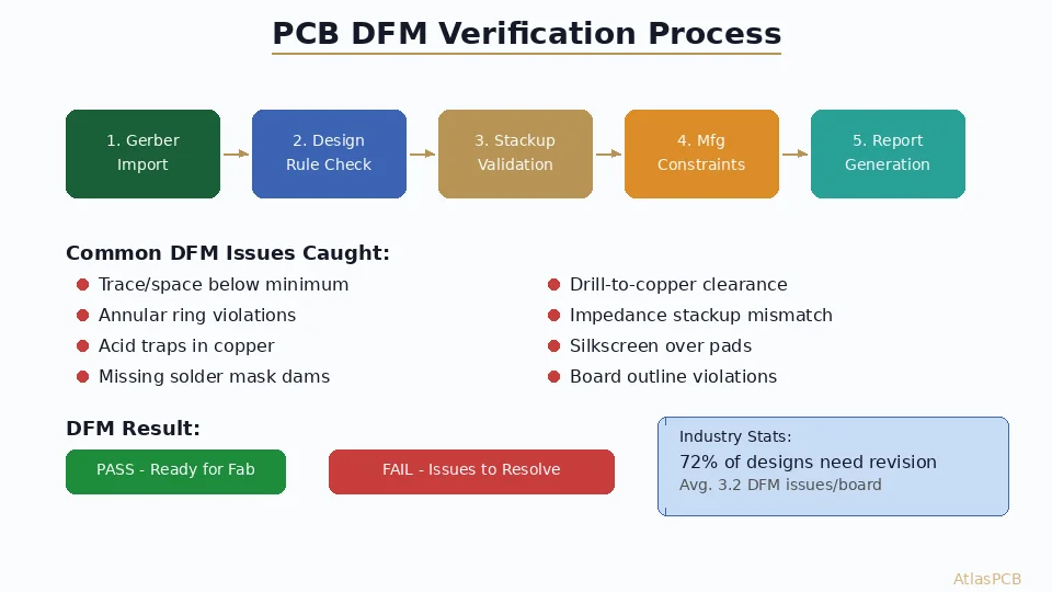
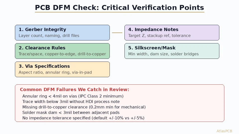
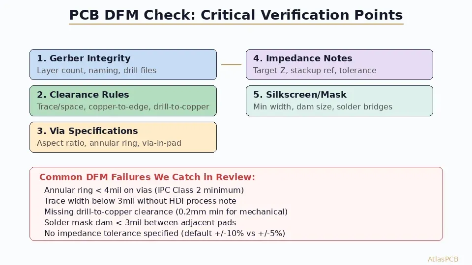
A proper PCB DFM check verifies five critical areas before fabrication: Gerber file integrity (all layers present, correct format, drill files included), clearance rules (trace-to-trace, copper-to-edge, drill-to-copper), via specifications (aspect ratio within process capability, annular ring meets IPC minimums), impedance specifications (target values, reference layers, tolerance), and solder mask/silkscreen (minimum dam width, text size, mask openings). Catching these issues before submission saves 3-7 days and $500-2000 per revision cycle.
Quick Reference: The 5-Point DFM Verification
| Check Point | What to Verify | Common Failure | Time to Fix |
|---|---|---|---|
| 1. Gerber Integrity | All layers present, correct format, drill files | Missing paste mask or wrong format | 30 min |
| 2. Clearance Rules | Trace/space, copper-to-edge, drill-to-copper | Copper too close to board edge | 1-4 hours |
| 3. Via Specifications | Aspect ratio, annular ring, via-in-pad | Annular ring below minimum | 2-8 hours |
| 4. Impedance Notes | Target Z, reference layers, tolerance | No stackup reference for impedance | 1 hour |
| 5. Mask/Silkscreen | Dam width, text size, opening accuracy | Solder bridges on fine-pitch | 1-2 hours |
Running through these five checks before submitting your Gerber package catches 78% of all DFM issues we see in production — saving an average of 4 days and one full board revision.
1. Gerber File Integrity: The Foundation
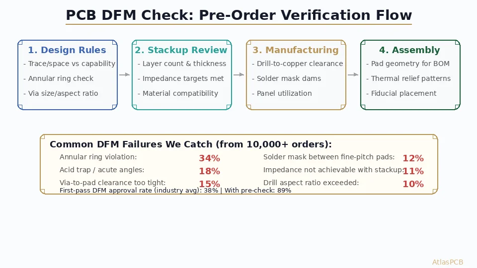
The most frustrating DFM rejection is a missing file. It sounds trivial, but 18% of our first-submission packages arrive incomplete — usually a missing paste mask layer, an outdated drill file from a previous revision, or a board outline that doesn’t match the copper layers.
Before zipping your Gerber package, open every file in a standalone viewer (not your EDA tool, which can display correct layers from its internal database even if the exported files are wrong). Verify the board outline matches on every layer, via locations align between drill files and copper pads, and that your drill file includes a complete tool table with the correct drill sizes. We’ve seen designs where the drill file references the previous revision’s tool table — resulting in 0.3mm holes drilled for 0.25mm pads, which fails annular ring instantly.
Naming convention matters more than you might think. When your fabricator receives files named “Layer1.gbr” through “Layer10.gbr” with no readme indicating which is top copper versus internal ground, they must guess based on aperture usage — and sometimes they guess wrong. Use explicit names: TopCopper.gbr, InnerGND1.gbr, InnerSig2.gbr, BottomCopper.gbr. The 30 seconds spent renaming prevents a 2-day misunderstanding.
ENGINEERING REVIEW
Upload Your Gerbers — We Check DFM Before Quoting
Our engineering team reviews every submission for manufacturability issues before production begins. Most problems caught within 4 hours of upload.
Upload Gerber Files ›
2. Clearance Rules: Where Designs Fail Silently
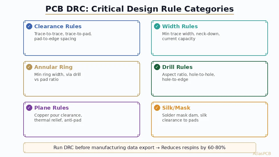
Clearance violations are insidious because your EDA tool may pass DRC with its own rules while the fabricator’s actual process capability is different. The most common disconnect: designers set 5mil trace/space in their rules (which many fabs can hit), but forget that copper-to-board-edge requires a separate, larger clearance — typically 0.25mm minimum for routed edges and 0.5mm for V-scored panels.
In our process engineering database, copper-to-edge violations account for 15% of all DFM holds. The failure mode is straightforward: during routing (mechanical separation of boards from panel), the router bit has a tolerance of +/-0.1mm. If your copper is at 0.15mm from the board edge, a routine routing deviation can expose copper on the edge — creating a short-circuit path or corrosion initiation site.
Drill-to-copper clearance is another silent killer, especially on dense designs. A plated through-hole needs clearance to adjacent inner-layer copper that accounts for both drill wander (+/-0.05mm typical for mechanical drills) and etch variation. Our minimum drill-to-copper clearance is 0.2mm for standard mechanical drilling and 0.15mm for laser-drilled microvias. Designs that push below these numbers may pass in simulation but fail on the panel when drill registration hits its worst-case tolerance.
3. Via Specifications: The Annular Ring Problem
Annular ring failures are the single largest category of DFM rejections we process — 23% of all manufacturing holds originate here. The root cause is a mismatch between the designer’s intent and the physical reality of drilling.
When you specify a 0.3mm drill with a 0.55mm pad, the nominal annular ring is 0.125mm (about 5mil). That sounds comfortable against IPC’s 1mil minimum. But factor in drill positional accuracy (+/-0.05mm), pad registration accuracy (+/-0.025mm per layer), and etch compensation variation (+/-0.015mm), and your actual annular ring on the fabricated board can be as low as 0.035mm (1.4mil). That’s close to the wire for IPC Class 2, and below minimum for Class 3.
The practical fix: design annular ring at minimum 4mil (0.1mm) for standard PTH vias in Class 2 applications, and 5mil (0.125mm) for Class 3. For BGA via-in-pad designs where pad size is constrained by pitch, use laser-drilled microvias (0.1mm drill) which have tighter positional accuracy (+/-0.025mm) and allow smaller annular rings.
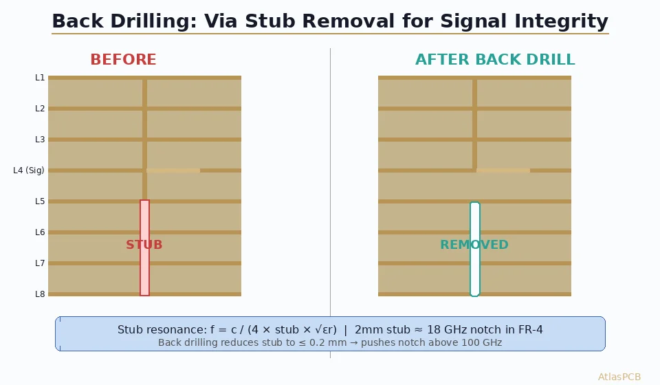
Via aspect ratio is the other critical check. Standard mechanical drilling supports aspect ratios up to 10:1 (depth-to-diameter). For a 1.6mm board, that means minimum 0.16mm drill diameter. Going below this ratio risks drill breakage, hole wall quality degradation, and plating voids in the barrel. If your design needs smaller vias in a thick board, you need either HDI laser drilling (sequential lamination) or back-drilling to reduce the effective aspect ratio.
HDI CAPABILITIES
Need Smaller Vias? HDI Solves Aspect Ratio Limits
Laser-drilled microvias from 0.075mm with 5+N+5 buildup capability. Via-in-pad with planarized fill for BGA escape routing.
Explore HDI Options ›4. Impedance Specifications: What Your Fabricator Needs
Specifying impedance without providing sufficient context is like ordering a machined part without tolerances — the result is undefined. Yet 10% of our DFM queries stem from incomplete impedance callouts. A proper impedance specification includes:
The target impedance value (e.g., 50 ohm single-ended, 100 ohm differential). The reference layer for each impedance class — because a 50-ohm microstrip on L1 referenced to L2 has a completely different trace width than 50-ohm stripline on L3 referenced to L2 and L4. The tolerance (standard +/-10%, tight +/-5%, precision +/-3%). And critically, whether you want the fabricator to adjust trace width to hit impedance (common) or hold your trace width and adjust dielectric thickness (rare but sometimes necessary for dense routing).
The most productive approach: provide your stackup intent (layer count, approximate dielectric thicknesses, copper weights) along with impedance targets, and let the fabricator’s process engineers optimize the final stackup for their materials and processes. They know their actual Dk values (which drift from datasheet by 2-5%) and their etch compensation factors. Trying to specify both the stackup AND the impedance without giving the fab room to adjust creates conflicts that delay production.
5. Solder Mask and Silkscreen: The Final Check
Solder mask issues rarely kill a design outright, but they cause assembly defects that are expensive to debug in production. The critical parameter is solder mask dam width — the sliver of mask material between adjacent pads. Below 3mil (75um), the mask tends to tear during development or lift during soldering, creating bridges between pads.
For BGA packages at 0.5mm pitch, the pad opening is typically 0.3mm (NSMD design), leaving only 0.2mm between adjacent openings for the mask dam. That’s 8mil — comfortable. But at 0.4mm pitch BGAs, the dam drops to 3-4mil, pushing fabrication limits. If your design uses 0.4mm pitch BGAs, verify with your fabricator that their LDI (laser direct imaging) equipment can reliably resolve the dam pattern — not all shops can.
Silkscreen is the least critical DFM element, but poorly placed reference designators that overlap pads or extend beyond the board outline create confusion during assembly inspection. A quick cleanup pass — removing designators under components and ensuring minimum 5mil text height for laser-marked legend — saves time in the assembly house.
IMPEDANCE CONTROLLED PCB MANUFACTURER
Engineering Review Catches 78% of DFM Issues
Don't guess if your design is manufacturable. Upload your files and our team provides a detailed DFM report — typically within 4 hours.
Submit for Review ›The DFM Checklist: Print and Use
Before every fabrication submission, walk through this sequence:
- Open all Gerber files in a standalone viewer — verify alignment, completeness, no blank layers
- Check copper-to-board-edge: minimum 0.25mm routed, 0.5mm V-scored
- Verify annular ring: minimum 4mil (Class 2) or 5mil (Class 3) on all via pads
- Confirm drill aspect ratio: diameter > board_thickness / 10 for mechanical drills
- Include impedance table with: target value, reference layer, tolerance, and whether width or stackup should flex
- Verify solder mask dam > 3mil between all adjacent pads
- Include a fabrication note file covering: material, surface finish, impedance, special requirements
This 15-minute verification catches most issues that would otherwise cost you a week of back-and-forth with engineering queries.
ATLASPCB
Ready to Order? Upload for Instant DFM Analysis
Our automated DFM system plus engineering review ensures your design is production-ready. Get quote and DFM report simultaneously — no back-and-forth delays.
Get Instant Quote ›
Reviewed by AtlasPCB Engineering Team — 15+ years in advanced PCB fabrication for RF, HDI, and rigid-flex applications.
Related Reading:
About AtlasPCB — We specialize in complex PCB manufacturing for HDI, RF, and high-reliability applications. Explore our free engineering DFM review . Every order includes free engineering review. Get your quote.
Reviewed by AtlasPCB Engineering Team — IPC-certified manufacturing specialists with 15+ years of production experience in HDI, RF, and high-reliability PCB fabrication. Content based on factory floor data and real customer design reviews.
Frequently Asked Questions
What are the most common DFM errors that cause PCB fabrication rejection?
What minimum annular ring does IPC require?
Should I include impedance requirements in my Gerber package?
How do I verify my Gerber files are complete before submitting?
- PCB DFM
- design for manufacturability
- Gerber files
- PCB fabrication
- clearance rules
- annular ring
- manufacturing