· David Okafor · Engineering · 8 min read
PCB Layer-to-Layer Registration
Complete guide to PCB layer-to-layer registration accuracy. Covers IPC Class 2 and Class 3 alignment tolerances, pin lamination vs mass lamination, X-ray registration systems, and design rules for achieving ±1 mil accuracy in HDI multilayer boards.
Quick Answer
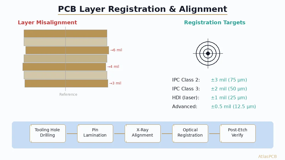
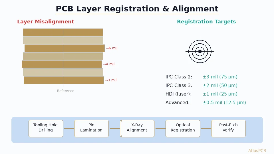
PCB layer-to-layer registration is the accuracy with which copper patterns on adjacent layers align relative to each other and to drilled holes. IPC-6012 Class 2 requires ±3 mil (75 μm) registration, Class 3 requires ±2 mil (50 μm), and advanced HDI processes achieve ±1 mil (25 μm) or better using X-ray alignment and laser-drilled registration targets.
What Is Layer-to-Layer Registration?
Layer-to-layer registration refers to the positional accuracy with which copper patterns on different layers of a multilayer PCB align relative to each other and to drilled through-holes. In a perfectly registered board, all layer features align exactly as designed. In practice, manufacturing variations introduce offsets that must be controlled within specified tolerances.
Registration accuracy directly impacts:
- Annular ring integrity: Misaligned layers cause drill breakout, reducing pad-to-hole contact
- Controlled impedance: Lateral trace shift relative to reference planes alters characteristic impedance
- Signal integrity: Differential pair symmetry degrades when layers shift asymmetrically
- Reliability: Reduced annular rings fail earlier under thermal cycling stress
- BGA fanout: Tight-pitch BGA routing relies on precise via-to-pad alignment
For modern designs running PCIe Gen5/6, DDR5, or 56G+ SerDes, registration tolerance is as critical as trace width control.
IPC Registration Standards and Requirements
IPC-6012 Registration Classes
The IPC-6012 standard defines minimum registration requirements based on product class:
Class 2 — Standard Commercial Electronics
- Layer-to-layer registration: ±3 mil (75 μm)
- Layer-to-drill registration: ±4 mil (100 μm)
- Suitable for consumer electronics, IoT devices, general-purpose boards
Class 3 — High Reliability
- Layer-to-layer registration: ±2 mil (50 μm)
- Layer-to-drill registration: ±3 mil (75 μm)
- Required for telecom, industrial, automotive, medical devices
Class 3/A — Aerospace/Military
- Layer-to-layer registration: ±1.5 mil (38 μm)
- Layer-to-drill registration: ±2 mil (50 μm)
- Space, defense, and life-critical applications
Advanced HDI (Beyond IPC Standard)
- Layer-to-layer registration: ±1.0 mil (25 μm)
- Laser via to pad: ±0.5 mil (12.5 μm)
- Semiconductor packaging substrates: ±0.3 mil (8 μm)
How Registration Tolerance Affects Design Rules
The relationship between registration tolerance and minimum feature sizes:
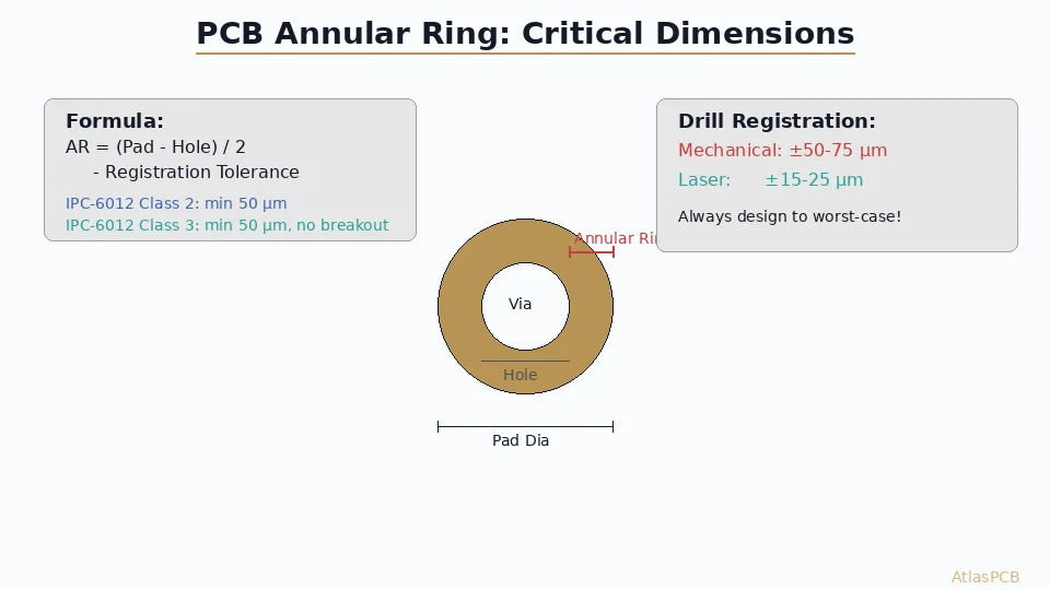
Minimum Annular Ring = (Pad Diameter - Drill Diameter) / 2 - Registration Tolerance
For example, with an 18 mil pad and 10 mil drill:
- Available annular ring = (18 - 10) / 2 = 4 mil
- Class 2 registration (±3 mil) → Effective minimum = 4 - 3 = 1 mil ⚠️ (barely acceptable)
- Class 3 registration (±2 mil) → Effective minimum = 4 - 2 = 2 mil ✓
This calculation demonstrates why tight-pitch designs often require Class 3 registration even for commercial products.
Manufacturing Methods for Registration Control
Pin Lamination (Standard Method)
Pin lamination is the most widely used registration method for multilayer PCBs:
- Tooling hole drilling: Precision holes drilled in each inner layer panel at fixed locations
- Pin alignment: Layers stacked on precision steel pins that pass through tooling holes
- Lamination press: Stack pressed under heat and pressure while pins maintain alignment
- Post-lamination drilling: Through-holes drilled using the same tooling hole reference
Achievable accuracy: ±2 to ±3 mil (50-75 μm)
Limitations:
- Tooling hole quality limits accuracy
- Material shrinkage during lamination introduces systematic offset
- Thermal expansion of pins during hot press cycle
- Panel warpage can cause local misalignment
Mass Lamination (High-Volume)
Used in high-volume Asian factories for standard consumer electronics:
- Slot/notch alignment: Layers indexed using edge slots rather than pins
- Optical pre-alignment: Camera systems verify alignment before press
- Rapid press cycle: High-throughput but slightly lower precision
Achievable accuracy: ±3 to ±4 mil (75-100 μm)
X-Ray Registration (High-Accuracy)
For HDI and high layer count boards, X-ray registration provides superior accuracy:
- X-ray targets: Special registration marks embedded in inner layers (copper targets)
- X-ray imaging: After lamination, X-ray system images internal targets through the panel
- Drill compensation: CNC drill program automatically compensates for measured offset
- Layer-specific correction: Each layer pair’s offset calculated independently
Achievable accuracy: ±1 to ±1.5 mil (25-38 μm)
Advantages:
- Compensates for post-lamination material movement
- Eliminates tooling hole dependency
- Enables independent correction for each drill span
- Required for 16+ layer builds and any-layer HDI
Laser Direct Imaging (LDI) with Registration
Modern LDI exposure systems can incorporate real-time registration compensation:
- Fiducial reading: Camera reads panel fiducials before exposure
- Image scaling: Digital artwork scaled to match actual panel dimensions
- Local correction: Different areas of the panel receive independent scaling
- Compensation data: Feed-forward from previous process steps
This approach addresses the material dimensional changes that occur during processing rather than just managing mechanical alignment.
Sources of Registration Error
Material Dimensional Instability
FR-4 base material changes dimensions during processing:
- After copper etching: Stress relief causes 0.02-0.05% shrinkage
- During oxide/alternative oxide: Thermal cycle causes 0.01-0.03% expansion
- During lamination: Compression and heat cause complex dimensional changes
- After reflow: Additional 0.01% dimensional change possible
For a 500 mm panel, a 0.03% dimensional change equals 150 μm (6 mil) — significant for registration.
Copper Pattern Influence
Non-uniform copper distribution causes anisotropic dimensional changes:
- Heavy copper areas resist material movement
- Sparse copper areas allow more shrinkage
- This creates localized registration shift (sometimes called “artwork shift”)
- Copper balancing helps maintain uniform dimensional stability
Process-Induced Errors
| Error Source | Typical Magnitude | Mitigation |
|---|---|---|
| Tooling hole accuracy | ±0.5 mil | Precision CNC drilling |
| Pin diameter tolerance | ±0.1 mil | Ground steel pins, regular calibration |
| Material shrinkage | 0.02-0.05% | Scaling compensation artwork |
| Thermal expansion (press) | Variable | Controlled ramp rates |
| Sequential lamination (per cycle) | +0.3-0.5 mil | X-ray registration |
| LDI exposure accuracy | ±0.3 mil | Regular calibration |
Tight Registration Requirements for Your HDI Design?
AtlasPCB achieves ±1 mil layer registration with X-ray alignment systems. We provide registration coupons on every panel for verification.
Request HDI Capabilities Review →Design for Registration: DFM Guidelines
Annular Ring Sizing Strategy
Design annular rings to accommodate worst-case registration:
Start with minimum copper annular ring required by IPC class
- Class 2: 2 mil minimum (external), 1 mil (internal)
- Class 3: 3 mil minimum (external), 2 mil (internal)
Add registration tolerance margin
- Add full registration tolerance value for a 100% yield target
- Add 75% for a practical ~99.7% yield target (3σ process)
Consider drill accuracy separately
- Mechanical drill: ±2 mil position accuracy
- Laser drill: ±0.5 mil position accuracy
- Total positional tolerance = √(registration² + drill²) for RSS method
Registration-Friendly Design Practices
Artwork Scaling Compensation
- Work with your fabricator to determine their standard scaling factors
- Typical inner layer artwork is scaled 1.0002-1.0005× to pre-compensate for shrinkage
- Some fabricators use predictive models based on copper density
Fiducial and Target Placement
- Place registration targets in panel frame area (4 corners minimum)
- Add targets within board outline for large boards (>300 mm)
- Use copper-cleared circular targets (1-2 mm diameter) visible to optical systems
Layer Pair Optimization
- Keep critical signal-reference pairs on the same core (laminated together)
- Avoid routing critical differential pairs on layers that span multiple sequential laminations
- Place highest-density BGA breakout on layers closest to the same core
Via Design for Registration Tolerance
For through-hole vias in Class 3 designs:
| Via Drill | Minimum Pad | Annular Ring (after plating) | Registration Budget |
|---|---|---|---|
| 8 mil | 16 mil | 4 mil | ±2 mil Class 3 |
| 10 mil | 18 mil | 4 mil | ±2 mil Class 3 |
| 12 mil | 20 mil | 4 mil | ±2 mil Class 3 |
| 6 mil (laser) | 10 mil | 2 mil | ±1 mil HDI |
Verification and Measurement
Registration Coupon Design
Include dedicated registration measurement coupons in the panel frame:
- Type 1 — Layer-to-layer: Targets on each layer pair measured by X-ray or cross-section
- Type 2 — Layer-to-drill: Targets around drilled holes measured by optical inspection
- Type 3 — Full registration map: Grid of targets across the panel for spatial uniformity data
Measurement Methods
- Microsection: Cross-section and measure under microscope (destructive, highest accuracy)
- X-ray inspection: Non-destructive measurement of internal target alignment
- Electrical test: Dedicated registration coupon with breakable connections at tolerance limits
- Automated optical inspection (AOI): Surface layer-to-drill registration check
Statistical Process Control
Leading fabricators track registration data in SPC charts:
- Cpk ≥ 1.33 indicates process capability meeting spec with margin
- Regular Gauge R&R studies validate measurement system
- Trend analysis predicts when tooling/calibration maintenance is needed
Impact on High-Speed Signal Integrity
Registration errors affect signal integrity in several ways:
Impedance Variation
A trace designed for 50Ω impedance on a 4 mil dielectric will see impedance shift if registration moves the trace laterally relative to its reference plane:
- 1 mil lateral shift: ~1-2% impedance change
- 2 mil lateral shift: ~3-5% impedance change
- 3 mil lateral shift: ~5-8% impedance change
Differential Pair Skew
When the signal layer registration differs from the reference plane registration, one trace of a differential pair may be closer to the reference plane than the other, creating:
- Propagation velocity imbalance
- Common-mode noise generation
- Effective skew equivalent to 1-3 ps per mil of registration error
Pad-to-Anti-pad Clearance
Via anti-pads (clearance holes in planes) must maintain adequate clearance even with registration error. If the via shifts but the anti-pad doesn’t (or vice versa), the plane copper encroaches on the barrel, creating capacitive loading or, in worst cases, a short circuit.
Related Design Considerations
- Annular ring standards: How registration tolerance feeds into pad sizing
- HDI stackup design: Sequential lamination and registration challenges
- Controlled impedance design: How alignment affects impedance control
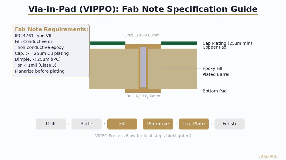
- Via-in-pad design: Registration requirements for VIPPO processes
Conclusion
Layer-to-layer registration is a foundational capability that constrains minimum feature sizes, determines pad geometries, and influences signal integrity margins. By understanding the registration capabilities of your chosen fabrication process — and designing with appropriate margins — you avoid yield-limiting annular ring violations and maintain the electrical performance your design requires.
For HDI and high layer count designs targeting ±1 mil registration, specify X-ray alignment in your fabrication notes and include registration measurement coupons. Work with fabricators who provide Cpk data demonstrating their registration process capability matches your design needs.
Designing a board with tight registration requirements? AtlasPCB’s HDI and multilayer capabilities include X-ray registration alignment systems achieving ±1 mil accuracy. We include registration coupon data in our quality reports. Upload your design for review →
About AtlasPCB — We specialize in complex PCB manufacturing for HDI, RF, and high-reliability applications. Explore our HDI PCB manufacturing capabilities, multilayer PCB fabrication up to 30 layers, or get an free engineering DFM review . Every order includes free engineering review. Get your quote.
Reviewed by AtlasPCB Engineering Team — IPC-certified manufacturing specialists with 15+ years of production experience in HDI, RF, and high-reliability PCB fabrication. Content based on factory floor data and real customer design reviews.
Frequently Asked Questions
What is the minimum annular ring needed to accommodate registration tolerance?
How does registration affect controlled impedance?
What causes registration to degrade in high layer count boards?
- layer registration
- PCB alignment
- multilayer PCB
- IPC tolerances
- HDI
- pin lamination
- X-ray alignment
- annular ring
- DFM
- manufacturing process