· AtlasPCB Engineering · Engineering · 12 min read
PCB Stackup Design Guide: How Layer Assignment and Material Choice Impact Cost, Signal Integrity, and Manufacturing
Practical guide to PCB stackup design covering layer assignment rules for mixed-signal boards, impedance planning, material selection trade-offs, and how stackup decisions directly impact manufacturing cost and lead time.
Quick Answer
Optimal PCB stackup design assigns high-speed signals adjacent to unbroken ground planes, separates analog from digital with a ground boundary, and uses symmetric copper distribution to prevent warpage — with 8-layer designs offering the best cost-to-performance ratio for mixed-signal boards requiring impedance control and crosstalk isolation.
Quick Answer: Layer Assignment Rules That Save Respins
| Rule | Rationale | Cost of Violation |
|---|---|---|
| High-speed signals adjacent to solid GND | Controlled impedance reference | 1-3 board respins |
| Analog and digital separated by GND plane | Prevents digital noise coupling to ADC | Signal integrity failure |
| Power planes paired in stackup center | Decoupling capacitance + thermal balance | EMI compliance failure |
| Symmetric copper distribution (top to bottom) | Prevents warpage during lamination | Yield loss, assembly issues |
| Signal layers use same prepreg thickness | Consistent impedance across all signal layers | Mixed impedance results |
The single most expensive stackup mistake we see — accounting for roughly 30% of customer redesigns that come through our engineering review — is placing high-speed differential pairs on a layer that lacks a continuous ground reference directly adjacent. Engineers route DDR5 byte lanes on layer 3 with a split power plane on layer 4, creating impedance discontinuities at every power domain boundary that no amount of post-layout simulation can fix without moving traces to a different layer.
The Fundamental Principle: Reference Plane Adjacency
Every transmission line needs a return current path. For a microstrip on the top layer, that return current flows on the adjacent ground plane directly below. For a stripline on an inner layer, return currents flow on both adjacent planes. The impedance of the transmission line — and therefore your signal integrity — depends on the geometric relationship between the signal trace and its reference plane remaining constant along the entire trace length.
When a signal trace crosses a split in its reference plane (a gap between 3.3V and 1.8V domains, for example), the return current must detour around the split. This detour creates a loop antenna that radiates, increases the effective inductance of the return path, and causes a local impedance spike that reflects energy back toward the driver. At DDR5 data rates (4800 MT/s and above), a single reference plane split under a byte lane creates enough impedance discontinuity to close the data eye below the receiver threshold.
In our production data from impedance-controlled boards, we consistently measure +/-3% impedance on traces with solid reference planes and +/-8-12% on traces that cross plane splits — even when the nominal trace geometry is identical. The difference is entirely attributable to the return path discontinuity affecting the effective dielectric height and field distribution.
The practical rule: signal layers in your stackup must be adjacent to either a solid ground plane or a power plane that has no splits under any signal routing path. If you must split a power plane, no high-speed signal on the adjacent layer should cross that split. This is a constraint that your stackup design must accommodate from the start — it cannot be fixed in layout without changing the layer assignment.
PCB STACKUP DESIGN GUIDE
Need Help With Your Stackup?
Our engineers design optimized stackups for impedance control, signal integrity, and manufacturability. Free stackup consultation with every quote.
Get Stackup Recommendation ›
8-Layer Mixed-Signal: The Workhorse Stackup
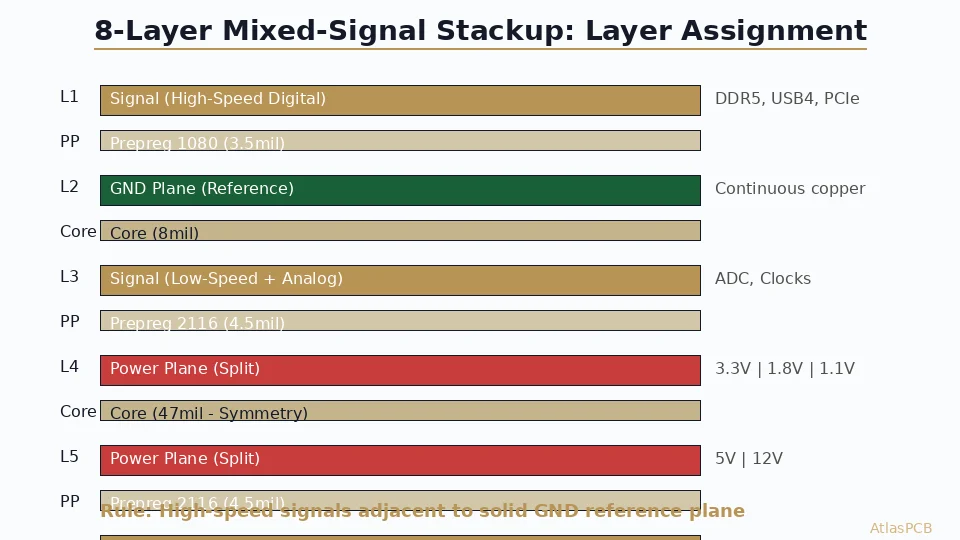
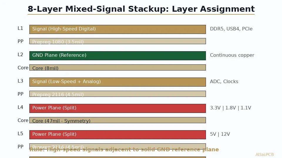
For designs combining high-speed digital interfaces (DDR4/5, USB3.2+, PCIe Gen4+) with sensitive analog circuitry (ADCs above 14 bits, RF receive chains, precision measurement), the 8-layer stackup provides the minimum layer count that allows proper isolation without forcing routing compromises.
The recommended layer assignment for an 8-layer mixed-signal board:
Layer 1 (Signal): High-speed digital — DDR byte lanes, USB differential pairs, PCIe lanes. This layer benefits from direct probe access during debug and has a solid ground reference on Layer 2.
Layer 2 (Ground): Continuous, unbroken ground plane. This is the impedance reference for Layer 1 and the shield between digital signals and the inner analog routing. No splits, no routing, no thermal reliefs that break continuity under signal traces.
Layer 3 (Signal): Secondary digital routing — slower interfaces, SPI, I2C, GPIO, and clock distribution that does not require the tightest impedance control. Alternatively, this layer serves low-frequency analog routing if proper separation from digital domains is maintained.
Layer 4 (Power): Split power plane for digital supplies — 1.1V core, 1.8V I/O, 3.3V peripherals. Plane splits are acceptable here because no high-speed signals reference this layer directly (Layer 3 references Layer 2 ground above it).
Layer 5 (Power): Analog power and secondary digital supplies — AVDD, VREF, 5V, 12V. Having separate analog power on a different layer from digital power prevents conducted noise coupling through shared copper.
Layer 6 (Signal): Sensitive analog signals — ADC inputs, sensor traces, RF intermediate frequency paths. Referenced to Layer 7 ground below, this layer is shielded from digital noise by the power planes above it.
Layer 7 (Ground): Second continuous ground plane. Provides impedance reference for Layer 6 analog signals and Layer 8 bottom-side routing.
Layer 8 (Signal): Bottom-side component routing, power delivery to components, and overflow digital routing. Referenced to Layer 7 ground.
This arrangement creates three distinct electromagnetic environments: Layers 1-2 for high-speed digital (shielded below by ground), Layers 6-7 for sensitive analog (shielded above by power planes), and the middle power planes as the boundary between domains. The ground plane on Layer 2 and Layer 7 are connected by stitching vias around the board perimeter and at strategic locations to ensure they remain at the same potential.
How Stackup Choices Drive Manufacturing Cost
The cost of a multilayer PCB is not simply proportional to layer count. The specific stackup configuration — materials, thicknesses, and construction method — can create 2-3x cost variation between two boards with identical layer counts. Understanding these cost drivers allows engineers to design stackups that achieve their electrical requirements without unnecessary manufacturing premiums.
Layer count itself adds 15-25% per layer pair (going from 6 to 8 layers, or 8 to 10 layers). This reflects additional copper foil, prepreg sheets, and lamination cycles. However, the incremental cost decreases as layer count increases — adding layers 7-8 to a 6-layer board costs proportionally more than adding layers 9-10 to an 8-layer board, because the fixed costs of panel handling and testing are already amortized.
Prepreg and core thickness specifications significantly impact cost when non-standard values are required. Standard prepreg offerings (1080 at 2.8 mil, 2116 at 4.5 mil, 7628 at 7.5 mil after pressing) are in stock at every fabricator. Requesting 1035 prepreg (1.5 mil) or thin cores below 3 mil enters specialty territory with longer lead times and 30-50% material premiums. Before specifying thin dielectrics for impedance targets, verify whether adjusting trace width on standard-thickness prepreg achieves the same impedance — it often does.
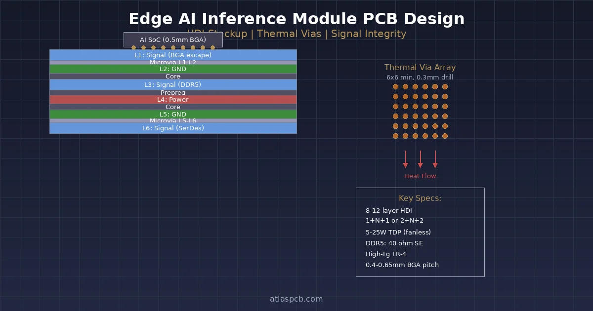
Sequential lamination (required for HDI buildup layers) adds a separate lamination, drilling, and plating cycle for each sequential stage. A 2+N+2 buildup costs approximately 40-60% more than a standard 8-layer board of the same total thickness, due to the additional processing steps and higher yield loss from multiple lamination alignments. This cost is justified when routing density requires microvias, but should not be specified when conventional through-hole vias can achieve the required breakout.
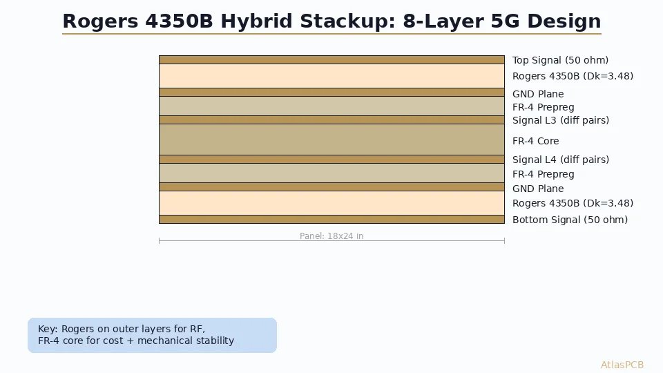
Material upgrades follow a tiered cost structure. Standard FR-4 (Tg 140-150) is the baseline. Mid-Tg FR-4 (Tg 170) adds 5-10%. High-performance laminates (Megtron 4, IS415) add 30-50%. Rogers or PTFE layers in a hybrid stackup add 3-5x for those specific layers plus a processing premium for hybrid lamination.
MULTILAYER PCB COST
Get Accurate Pricing for Your Stackup
Upload your design and stackup specification. We provide detailed cost breakdown showing exactly where your budget goes.
Compare Pricing Options ›Impedance Planning in Stackup Design
Impedance control starts with stackup design, not trace width calculation. The target impedance values (50 ohm single-ended, 90 or 100 ohm differential) constrain the relationship between trace width, dielectric height, and dielectric constant. Choosing the dielectric height during stackup planning determines what trace widths will be required — and trace width directly impacts routing density.
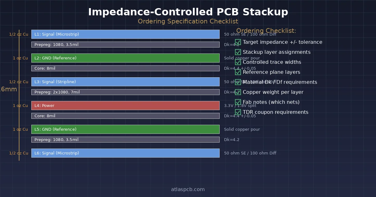
For a 50-ohm microstrip on standard FR-4 (Dk=4.3), the approximate relationships are: 5 mil trace requires 3.2 mil dielectric height, 4 mil trace requires 2.5 mil dielectric height, 3 mil trace requires 1.8 mil dielectric height. If your routing density requires 4 mil traces (for BGA breakout, for example), your stackup must provide approximately 2.5 mil dielectric height on that signal layer — which typically means a single 1080 prepreg sheet pressed to specification.
Differential pairs have an additional constraint: the pair spacing (edge-to-edge) interacts with the dielectric height to determine both the differential impedance and the common-mode impedance. Tight coupling (spacing less than 2x trace width) provides better noise rejection but requires wider traces to maintain impedance, consuming more routing space. Loose coupling (spacing greater than 3x trace width) acts approximately like two independent 50-ohm traces but provides less common-mode rejection.
We recommend that engineers specify target impedances to their PCB manufacturer early in the design process and receive a stackup recommendation before beginning layout. Our process engineers run impedance simulations using actual measured material properties (not catalog Dk values) and provide trace widths calibrated to our process capability. This prevents the scenario where an engineer designs with catalog values, completes layout, and discovers during fabrication review that actual trace widths need to change by 0.5-1 mil to hit targets — potentially breaking spacing rules throughout the design.
Symmetric Copper Distribution: Preventing Warpage
PCB lamination involves heating the entire stackup to 180-200 C, applying 300-500 PSI pressure for 60-90 minutes, then controlled cooling. During this process, copper and dielectric materials expand and contract at different rates (CTE mismatch). If the copper distribution is symmetric from the board center outward, these thermal stresses balance and the finished board remains flat. Asymmetric copper creates differential stress that manifests as warpage — potentially exceeding the 0.75% limit specified by IPC-A-600 for surface mount assembly.
The practical guideline: each layer pair (equidistant from the board center) should have approximately equal copper coverage. Layer 1 should match Layer 8, Layer 2 should match Layer 7, and so on. If your design naturally places heavy ground planes on layers 2 and 7 (symmetric), and signal routing with 40-50% copper fill on layers 3 and 6 (also symmetric), warpage will be minimal.
Problems arise when designers place dense power planes on one side of the stackup center and sparse signal routing on the other. A layer with 85% copper coverage (ground plane) paired with a layer at 30% copper coverage (sparse routing) creates sufficient asymmetric stress to warp boards measurably. Our CAM engineers flag this during DFM review and recommend copper fill additions (thieving) to balance the distribution — but this is far easier to address during stackup planning than after layout completion.
For boards where warpage control is critical (large boards over 200mm, thin boards under 1.0mm, or boards with high-mass BGA components), we recommend targeting less than 15% copper coverage differential between paired layers. This sometimes means adding non-functional copper fill to routing layers or strategically sizing power plane splits to maintain balance.
IMPEDANCE CONTROLLED PCB MANUFACTURER
Stackup Design Assistance Included
Every impedance-controlled order includes stackup optimization by our process engineers. Calibrated trace widths, balanced copper, and verified dielectric heights.
Common Stackup Mistakes and Their Consequences
Beyond the reference plane adjacency issue, several stackup design errors appear repeatedly in our engineering review queue. Understanding these patterns helps engineers avoid them in new designs.
Using the same prepreg between all layers regardless of impedance requirements leads to trace widths that vary across signal layers — making routing rules inconsistent and confusing for layout engineers. Instead, choose prepreg thicknesses that allow a single trace width to achieve your target impedance on every signal layer. This means the prepreg between L1 and L2 might be different from the prepreg between L3 and L4 if L1 is microstrip and L3 is stripline.
Specifying overall board thickness without specifying individual layer thicknesses gives the fabricator freedom to choose any prepreg combination that achieves the total — but the resulting impedance might not match your simulation. Always specify the complete stackup with individual dielectric thicknesses, not just the total board height.
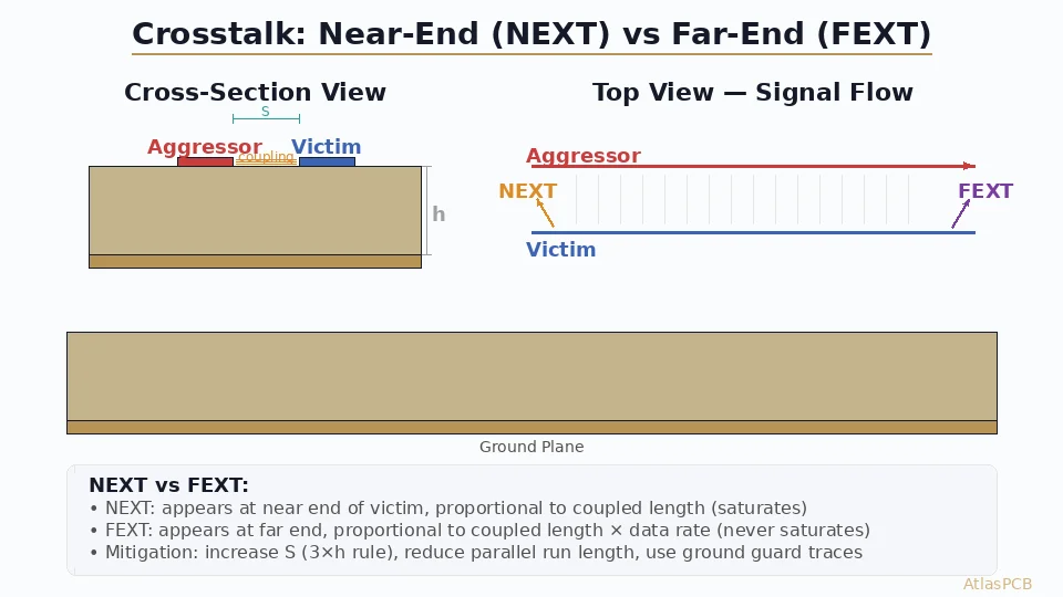
Placing two signal layers adjacent to each other (without a ground plane between them) creates broadside-coupled crosstalk that cannot be managed through spacing rules alone. The coupling coefficient between traces on adjacent layers at typical 4-5 mil separation exceeds -20 dB across wide bandwidth — meaning every trace on one layer injects noise into the nearest trace on the adjacent layer. This is particularly destructive for mixed analog/digital designs where a 10 MHz clock on one layer couples directly into a 16-bit ADC input on the layer below.
ATLASPCB
Design Confidence Starts With the Right Stackup
Upload your schematic constraints and target impedances. Our engineers return a complete, optimized stackup within 24 hours — ready for layout.
Request Stackup Design ›
Reviewed by AtlasPCB Engineering Team — 15+ years in advanced PCB fabrication for RF, HDI, and rigid-flex applications.
Related Reading:
About AtlasPCB — We specialize in complex PCB manufacturing for HDI, RF, and high-reliability applications. Explore our impedance-controlled PCB manufacturing . Every order includes free engineering review. Get your quote.
Reviewed by AtlasPCB Engineering Team — IPC-certified manufacturing specialists with 15+ years of production experience in HDI, RF, and high-reliability PCB fabrication. Content based on factory floor data and real customer design reviews.
Frequently Asked Questions
How do I choose between 6-layer and 8-layer PCB stackup?
What is the most cost-effective PCB stackup for impedance control?
Should high-speed signals be on outer or inner layers?
How does stackup design affect PCB manufacturing cost?
- pcb-design
- stackup-design
- impedance-control
- signal-integrity