· Marcus Lin · Engineering · 11 min read
RF PCB Design-to-Manufacturing Handoff: DFM Checklist for Rogers and PTFE Laminates
The complete DFM handoff checklist for RF PCB designs using Rogers 4350B, RO4003C, PTFE, and hybrid stackups. Covers the 12 most common handoff failures that cause respins, with specific tolerances and callouts your fab needs to build it right.
Quick Answer
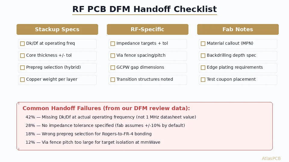
The most critical RF DFM handoff items are: specify Dk and Df at your actual operating frequency (not 1 MHz datasheet values), call out material by manufacturer part number (not just 'Rogers'), define impedance tolerance per layer (not one blanket spec), and include a test coupon plan. 42% of RF PCB respins we see trace back to missing or incorrect Dk specifications in the fab notes.
Quick Reference: The 12-Item RF DFM Handoff Checklist
| Item | What to Specify | Why It Matters |
|---|---|---|
| 1. Material MPN | Exact vendor P/N per layer | Prevents substitution |
| 2. Dk at operating freq | Value + frequency + source | Impedance accuracy |
| 3. Df at operating freq | Value + frequency | Loss budget verification |
| 4. Core thickness + tol | Nominal + acceptable range | Impedance sensitivity |
| 5. Copper weight/type | Weight + treatment (ED/RA/LoPro) | Roughness affects loss |
| 6. Impedance per layer | Target + tolerance + ref layer | Controlled manufacturing |
| 7. Via fence spec | Pitch + diameter + connection | Isolation guarantee |
| 8. Bonding material | Prepreg type for hybrid builds | CTE match + Dk continuity |
| 9. Backdrilling | Depth + stub length tolerance | Via resonance control |
| 10. Test coupon plan | Location + structure type | Verification method |
| 11. Edge plating | Where + thickness + continuity | EMI shielding |
| 12. Transition notes | Via anti-pad, clearance, routing | Signal integrity at transitions |
Why RF Handoffs Fail More Than Digital
RF PCB fabrication is fundamentally different from digital board manufacturing, even though they share the same basic process steps (lamination, drilling, plating, etching). The difference is sensitivity: a 50-ohm microstrip on FR-4 at 100 MHz can tolerate 15% variation in dielectric thickness without measurable performance degradation. The same trace at 28 GHz on Rogers will show 1.5 dB extra insertion loss and 6-ohm impedance shift from just 5% Dk variation.
In our facility, we track root causes for every RF board that requires a respin or revision. Over the past 18 months across approximately 500 RF board orders, the data consistently shows that the majority of failures trace back not to the manufacturing process itself, but to incomplete or ambiguous information in the design handoff package. The fab did what was specified — the specification was just wrong or incomplete.
The fundamental issue is that most EDA tools and stack designers assume “ideal” material properties, while fabrication deals with real material lots that have batch-to-batch variation, temperature-dependent properties, and process-induced changes to copper roughness and dielectric thickness. A proper handoff package bridges this gap by telling the manufacturer exactly what the design assumes and what tolerances are acceptable.
RF PCB ENGINEERING REVIEW
Not Sure Your Handoff Package is Complete?
Our RF team reviews your Gerbers, stackup, and fab notes before quoting. We'll flag missing specs that would cause problems in production.
Submit for Review ›
Material Specification: Getting Dk and Df Right
The 1 MHz Problem
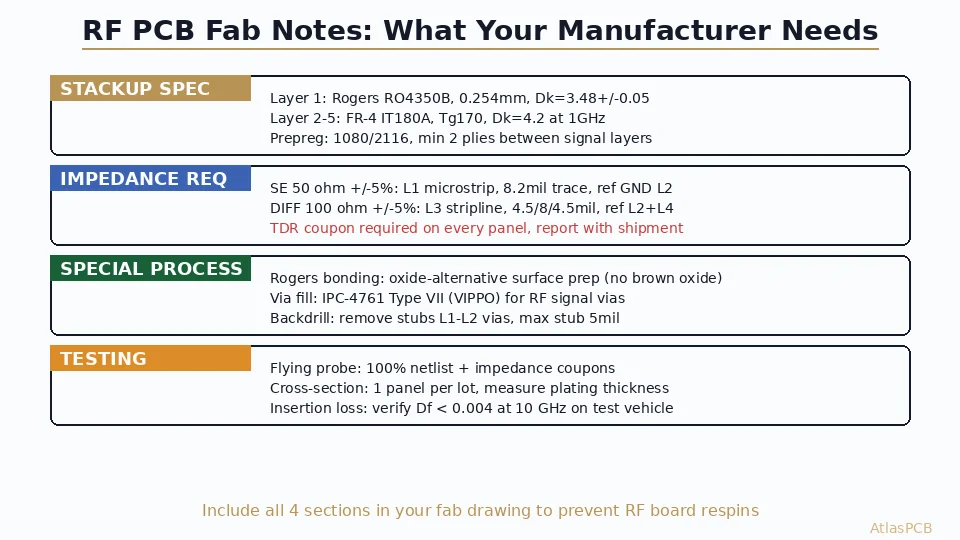
The single most common RF DFM failure we encounter — accounting for 42% of respins in our data — is specifying dielectric constant at the wrong frequency. Rogers and other laminate vendors publish Dk at multiple frequencies in their datasheets, but many designers (and some EDA tools) default to the 1 MHz value because that’s what IPC-TM-650 2.5.5.3 measures by default.
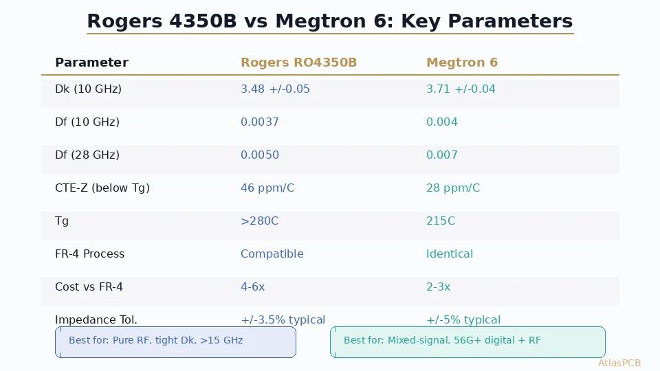
Here’s why this matters: Rogers RO4350B has a Dk of approximately 3.66 at 1 MHz (per IPC test method) but 3.48 at 10 GHz (per manufacturer’s clamped stripline resonator method). If you design a 50-ohm microstrip using Dk = 3.66, your trace will be narrower than optimal. The manufactured board (which actually sees Dk = 3.48 at your operating frequency) will have impedance approximately 3-4 ohms higher than target. On a single trace this might be acceptable — but across a matched filter network or phased array feed, it’s a specification failure.
The correct approach: specify Dk at or near your operating frequency, cite the measurement method, and state explicitly what Dk value your impedance calculation assumed. This lets the manufacturer verify that their incoming material lot (which they measure by resonator method) will produce the impedance you expect.
Copper Roughness and Its Effect on Dk
Another subtlety that causes problems: the effective Dk that your signal sees depends not just on the bulk laminate properties but also on copper surface roughness. Standard electrodeposited (ED) copper has an RMS roughness of approximately 5-7 um on the drum side, while Rogers LoPro (reverse-treated) copper reduces this to approximately 1.5-2 um.
At frequencies above 10 GHz, this roughness difference changes the effective Dk by 3-5% and can add 0.5-1.5 dB/inch of additional loss. If your impedance model doesn’t account for copper roughness (many don’t), and the fab uses standard ED copper instead of LoPro, your impedance will be off even if every other parameter is perfect.
Our recommendation: always specify copper type in your material callout. For designs above 10 GHz, call out “LoPro” or “HVLP” (Hyper Very Low Profile) explicitly. Below 5 GHz, standard ED copper is typically fine, but document the assumption.
Impedance Specification: Per-Layer, Not Blanket
Why Blanket Specs Waste Money or Cause Failures
A common pattern in fab notes: “All impedance-controlled traces: 50 ohm +/-10%.” This is problematic for two reasons. First, if your RF layers actually need +/-5% but your digital layers only need +/-10%, the blanket +/-10% spec means your RF layers aren’t controlled tightly enough. Second, if you specify +/-5% everywhere (to be safe for RF), you’re paying for tight control on digital layers that don’t need it — and potentially creating a situation where the fab cannot achieve your spec on internal FR-4 layers where Dk variation is inherently larger.
The professional approach is a layer-by-layer impedance table:
| Layer | Net Class | Target Z | Tolerance | Trace W | Ref Layer | Material |
|---|---|---|---|---|---|---|
| L1 | RF_50 | 50 ohm SE | +/-5% | 12.8 mil | L2 (GND) | RO4350B |
| L1 | RF_GCPW | 50 ohm GCPW | +/-5% | 10.2 mil | L2 + coplanar | RO4350B |
| L3 | USB3 | 90 ohm diff | +/-10% | 4.5/4.5 mil | L2,L4 | FR-4 |
| L5 | DDR4 | 40 ohm SE | +/-10% | 5.0 mil | L4,L6 | FR-4 |
This table tells the manufacturer exactly what matters and what doesn’t. They can focus process control budget on the layers that need it, potentially reducing cost while improving performance where it counts.
IMPEDANCE-CONTROLLED MANUFACTURING
+/-5% Impedance on RF Layers, Verified by TDR
Every RF board ships with impedance test report. Rogers, PTFE, and hybrid stackups — built by engineers who understand your frequency targets.
Hybrid Stackup Bonding: The Forgotten Specification
When building Rogers/FR-4 hybrid stackups, the bonding layer between dissimilar materials is a critical specification that 18% of designers in our data set completely omit from their fab notes. The prepreg or bonding film that joins a Rogers core to an FR-4 core determines:
CTE matching at the boundary. Rogers RO4350B has a Z-axis CTE of approximately 32 ppm/C below Tg, while standard FR-4 prepreg ranges from 50-70 ppm/C. This mismatch creates stress at the boundary during thermal cycling. The solution is either a low-CTE prepreg (such as Rogers RO4450F bondply) or standard 1080/2116 FR-4 prepreg with controlled glass content.
Dk at the boundary. If you have a controlled-impedance trace on the Rogers layer referencing a ground plane through a bonding layer, the Dk of that bonding material matters for your impedance calculation. Standard FR-4 prepreg (Dk approximately 4.0-4.2) is very different from Rogers bondply (Dk approximately 3.54). Your impedance model must use the correct value for whichever bonding material is specified.
Press temperature and time. Rogers materials have different lamination requirements than FR-4. RO4350B can use standard FR-4 press profiles (180-190C, 60-90 min), which is why it’s so popular for hybrid builds. But PTFE materials (RO5880, RO3003) require modified profiles — higher temperature, longer dwell, or sodium-etch surface preparation for adhesion. If your fab notes don’t specify the bonding approach, the manufacturer guesses. Sometimes they guess wrong.
Our standard practice for hybrid builds: we confirm the bonding material selection with the designer before fabrication and provide a cross-reference showing actual Dk at the bond layer versus what the impedance model assumes. This catches mismatches before they become expensive problems.
Via Fence and Isolation: Getting the Pitch Right
For RF designs above 10 GHz, via fencing (rows of ground vias surrounding signal traces) provides isolation and prevents parallel-plate mode propagation. The via fence pitch must be less than lambda/4 at the highest frequency of concern to prevent waveguide mode leakage.
The common mistake: designers use the same via pitch they’d use for digital ground stitching (40-60 mil / 1-1.5mm) and assume it works for RF isolation. At 28 GHz (lambda approximately 10.7mm in RO4350B), the maximum via pitch for effective shielding is approximately 2.5mm. At 77 GHz (automotive radar), it drops to approximately 0.9mm — which requires laser-drilled vias because mechanical drill tooling at 0.3mm diameter with 0.9mm pitch is at the edge of manufacturing capability.
When specifying via fences in your fab notes, include: via diameter, center-to-center pitch, connection (whether each via connects to both top and bottom ground, or just one side), and whether backdrilling is required (for thick stackups where via stubs could resonate).
EXPERT RF FABRICATION
Via Fencing, Backdrilling, Edge Plating — We Handle the Details
Our process engineers review every RF board for isolation adequacy and via resonance before production. From 2.4 GHz WiFi to 77 GHz radar.
Start RF Project ›Test Coupon Strategy: Verifying What Matters
Test coupons are your insurance policy on RF boards. But generic impedance coupons may not tell you what you need to know. For RF designs, consider these coupon types:
Standard impedance coupon: Verifies that the manufacturing process achieves target impedance for each controlled net class. Place on the same panel, same layer position, same orientation as your actual traces. A coupon on a different panel or at a different location on the same panel may see slightly different press conditions.
Through-loss coupon (TRL structure): For designs above 10 GHz where insertion loss matters, a through-reflect-line coupon set lets you de-embed connector effects and measure actual per-inch loss. Specify the line length (typically 1-2 inches for the through, 0.5 inch for the reflect, and a line that’s lambda/4 longer than the through at your center frequency).
Isolation coupon: Two parallel traces with via fencing, separated by your minimum isolation distance. Measure coupling (S21) at your operating frequency to verify that via fence effectiveness matches simulation.
The key rule: specify coupon location as “on production panel, within 2 inches of board array.” Coupons at panel edges see different press pressure and temperature and don’t represent your board’s actual conditions.
The Complete Handoff Package: What to Send Your Manufacturer
A professional RF PCB handoff package contains more than Gerbers and a drill file. Here’s what should be included:
- Gerber files (RS-274X or Gerber X2) — all layers including fabrication drawing
- Drill files — separate for mechanical and laser drilling
- Stackup drawing — with material MPNs, Dk/Df values at frequency, copper weights, and thicknesses with tolerances
- Impedance table — per-layer targets as described above
- IPC netlist — for electrical test verification
- Fab notes document — material substitution policy (none without approval), via fill requirements, surface finish, marking
- Test requirements — impedance coupons, cross-section locations, ionic contamination limits
- Critical dimension callout — any features that need tighter tolerance than standard process (edge clearances, hole position tolerance on RF connectors)
Missing any of these for an RF board is like submitting an incomplete building permit — you’ll get questions at best, incorrect assumptions at worst.
ATLASPCB
Upload Your RF Design — We'll Verify the Handoff
Our engineering team checks every RF submission for DFM completeness before manufacturing starts. Dk verification, stackup feasibility, via fence adequacy — all reviewed by RF-experienced process engineers.
Upload RF Design ›
Reviewed by AtlasPCB Engineering Team — 15+ years in advanced PCB fabrication for RF, HDI, and rigid-flex applications.
Related Reading:
About AtlasPCB — We specialize in complex PCB manufacturing for HDI, RF, and high-reliability applications. Explore our RF and high-frequency PCB services, Rogers RO4350B PCB manufacturing, or get an impedance-controlled PCB manufacturing . Every order includes free engineering review. Get your quote.
Reviewed by AtlasPCB Engineering Team — IPC-certified manufacturing specialists with 15+ years of production experience in HDI, RF, and high-reliability PCB fabrication. Content based on factory floor data and real customer design reviews.
Frequently Asked Questions
What Dk value should I specify for Rogers 4350B in my fab notes?
How do I specify impedance tolerance for RF layers vs digital layers?
What material callout format prevents fabrication errors?
Should I include test coupons in my RF PCB design?
What are the most common RF DFM handoff mistakes?
- RF PCB design and manufacturing
- PCB DFM check
- Rogers 4350B stackup
- China RF PCB manufacturer
- impedance controlled PCB manufacturer