· Priya Nair · Engineering · 6 min read
Solder Thermal Interface Materials (sTIMs) for AI
Explore how indium-based solder thermal interface materials (sTIMs) with 86 W/mK conductivity are solving AI processor thermal challenges. Learn about vacuum formic acid reflow, voiding minimization, and how PCB substrate design must evolve to support next-generation thermal solutions for data center AI accelerators.
Quick Answer
Indium-based solder thermal interface materials (sTIMs) achieve 86 W/mK thermal conductivity — 20-50× better than polymer TIMs (2-5 W/mK) — by forming metallurgical bonds between die and heat spreader. New vacuum formic acid reflow processes demonstrated at ECTC 2026 minimize voiding below 2% in large-area BGA packages, enabling uniform heat dissipation across 800mm² AI processor dies. PCB substrates supporting these packages must handle increased thermal cycling stress from the rigid sTIM connection and require enhanced via reliability for power delivery to 700W+ AI accelerators.
The AI Thermal Crisis and Why Polymer TIMs Are Failing
Every generation of AI accelerators pushes thermal design power (TDP) higher. NVIDIA’s B200 at 1000W, AMD’s MI400 series approaching 800W, and Intel’s Gaudi 3 at 600W — all concentrated in die areas under 900mm². The resulting heat flux exceeds 100 W/cm², pushing junction temperatures dangerously close to silicon’s reliability ceiling.
Between the die and the heat spreader sits a thin layer of thermal interface material — and at 100+ W/cm², the choice of TIM determines whether the chip operates reliably or throttles under thermal constraints.
At the 76th IEEE Electronic Components and Technology Conference (ECTC 2026, May 26-29, Orlando), Indium Corporation presented breakthrough research on solder thermal interface materials that may reshape how the industry approaches AI chip packaging — and by extension, how PCB substrates must evolve to support these solutions.
From Grease to Metallurgical Bonds: The sTIM Advantage
Thermal Conductivity Comparison
| TIM Type | Conductivity (W/mK) | Bond Line (µm) | Resistance (°C·cm²/W) | Reliability |
|---|---|---|---|---|
| Thermal grease | 2-8 | 25-50 | 0.03-0.25 | Pump-out risk |
| Phase change | 3-6 | 15-30 | 0.025-0.10 | Stable |
| Gap pad | 1-5 | 100-500 | 0.1-5.0 | Compression set |
| Graphite sheet | 10-20 (in-plane) | 25-100 | 0.01-0.05 | Delamination |
| Indium sTIM | 86 | 25-75 | 0.003-0.009 | Metallurgical |
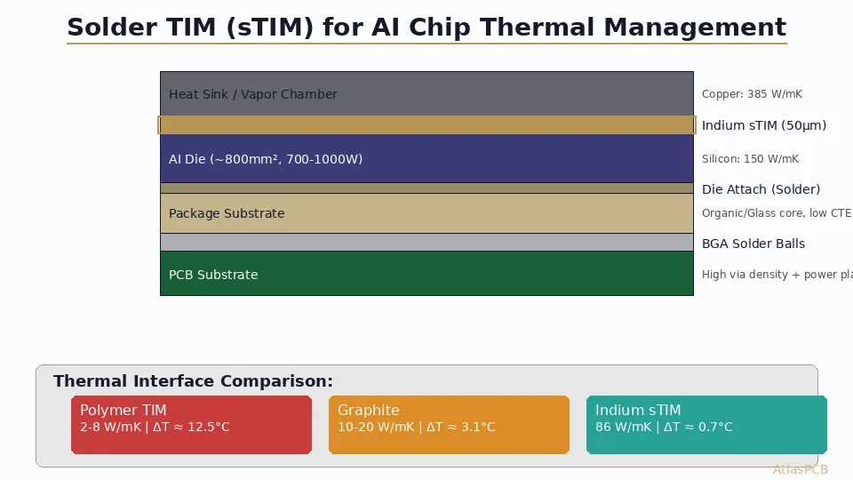
The 86 W/mK conductivity of indium sTIMs provides a 10-40× improvement in thermal resistance versus polymer alternatives. For an 800mm² die at 1000W:
Polymer TIM (5 W/mK, 50µm BLT): ΔT = 1000 × 0.005/(5 × 8) = 12.5°C
Indium sTIM (86 W/mK, 50µm BLT): ΔT = 1000 × 0.005/(86 × 8) = 0.7°C
That 11.8°C difference translates directly to either lower junction temperature (longer chip life) or higher allowable TDP (more compute performance).
Why Indium?
Indium (In) has unique properties that make it ideal for TIM applications:
- Low melting point: 156.6°C (compatible with multi-reflow assembly)
- High thermal conductivity: 86 W/mK (vs 50 for Sn, 62 for In-Sn eutectic)
- Exceptional ductility: Absorbs CTE mismatch strain without cracking
- Self-healing: Indium cold-welds under compression, sealing micro-cracks
- Low elastic modulus: 11 GPa (soft, doesn’t stress the die)
PCB Substrates for AI Accelerator Packaging
AtlasPCB manufactures high-layer-count substrates with enhanced via reliability and thermal management for AI hardware. Low-CTE materials, 700W+ power delivery, and 3000-cycle thermal endurance.
Explore Our Capabilities →ECTC 2026 Research: Fluxless Vacuum Formic Acid Reflow
The Voiding Challenge
Solder TIMs are only as good as their contact area. Any void (gas bubble) trapped at the interface creates a local thermal bottleneck — heat must conduct around the void, creating hot spots that can exceed damage thresholds.
For a 800mm² AI die, even 5% voiding creates hot spots with 20× the average heat flux. The ECTC research targets are clear: voiding must stay below 2% for reliable AI chip operation.
Process Innovation
The vacuum formic acid reflow process presented at ECTC 2026 solves three problems simultaneously:
1. Oxide Removal Without Flux Formic acid vapor (HCOOH) reduces copper and indium surface oxides at temperatures above 150°C:
CuO + 2HCOOH → Cu(OOCH)₂ + H₂O → Cu + 2CO₂ + H₂O (at T>200°C)
InO₃ + 3HCOOH → In(OOCH)₃ + 3/2 H₂O → In + 3CO₂ + 3/2 H₂O
This eliminates flux residue trapped between die and heat spreader — a critical reliability concern since no cleaning is possible after lid attachment.
2. Vacuum Void Elimination Reflowing under vacuum (<100 Pa) prevents gas entrapment. Any gas generated during oxide reduction is evacuated rather than trapped as voids. The research demonstrates consistent voiding below 2% across the full bond area.
3. Multi-Reflow Compatibility AI packages undergo multiple reflow cycles:
- Die attach to substrate (first reflow)
- Lid attach with sTIM (second reflow)
- BGA ball attach to PCB (third reflow)
The vacuum formic acid process maintains void levels through multiple thermal cycles — critical for real manufacturing workflows.
Results and Implications
The Indium Corporation research (ECTC Paper Session) demonstrated:
- Voiding: <2% consistently across 20+ test samples
- Thermal resistance: 0.004 °C·cm²/W (near theoretical minimum for 50µm indium)
- Reliability: Survived 1000 thermal cycles (-40 to +125°C) without degradation
- Scalability: Process validated for package areas up to 2500mm²
PCB Substrate Design Implications
Increased Thermal Cycling Stress
Traditional polymer TIMs act as compliant layers that absorb CTE mismatch between silicon die (2.6 ppm/°C) and heat spreader (copper: 17 ppm/°C, vapor chamber: 8-12 ppm/°C). Solder TIMs, being rigid metallurgical connections, transfer this strain to other interfaces in the package stack.
The BGA solder joints between the package and PCB substrate now see increased cyclic strain:
- Silicon die → sTIM → copper lid: nearly rigid stack
- CTE mismatch concentrated at BGA joints and substrate
- Package warpage changes under thermal load
Substrate design response:
- Use low-CTE core materials (2-4 ppm/°C glass-ceramic or silicon)
- Increase BGA pad diameter for larger joint volume
- Specify underfill with optimized CTE matching
- Design for corner BGA joint strain (maximum distance from neutral point)
Power Delivery for 700W+ Processors
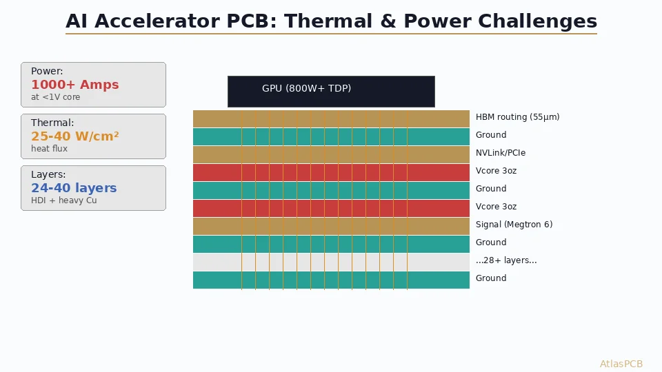
AI accelerators at 700-1000W draw 500-800A at sub-1V core voltage. The PCB substrate must deliver this current with minimal IR drop and inductance:
- Power plane copper: 2oz+ on dedicated power layers
- Via arrays: Hundreds of power vias in parallel (each carrying 2-5A)
- Decoupling: Embedded capacitors in substrate for high-frequency PDN response
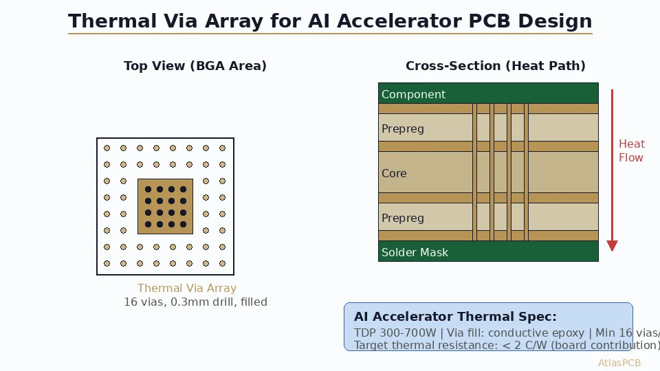
- Thermal vias: Separate thermal via arrays for heat extraction to PCB backside
Via Reliability Requirements
Data center AI servers operate continuously for 5+ years with 1000+ thermal cycles from power cycling and workload transitions. Substrate vias must survive:
- 3000+ thermal cycles (accelerated) without resistance increase
- Continuous 150°C operation (junction heat conducted through substrate)
- High current density (electromigration consideration for power vias)
Design strategies include:
- Maximum aspect ratio 6:1 for power vias
- Copper-filled (not plated-through) vias for minimum resistance
- Stacked microvia structures (shorter individual segments, higher reliability)
- Redundant via connections (no single via carrying more than 5A)
Industry Trajectory: Where sTIMs Lead PCB Substrate Design
Near-Term (2026-2027)
- sTIMs adopted for highest-performance AI accelerators (>800W)
- Organic substrates enhanced with low-CTE cores
- Via-in-pad filled with copper becomes standard for power delivery
Mid-Term (2028-2029)
- Glass core substrates (Intel Clearwater Forest approach) provide 3.2 ppm/°C CTE match
- Co-packaged optics add thermal constraints to substrate edges
- 2000W+ multi-chip modules require substrate-integrated liquid cooling channels
Long-Term (2030+)
- Silicon or glass interposers replace organic substrates for top-tier AI
- sTIM technology extends to chiplet-to-interposer bonds
- PCB substrate role shifts to power delivery and mechanical support
Practical Takeaways for Hardware Engineers
- If designing AI accelerator boards: Specify substrate materials with z-axis CTE below 15 ppm/°C and validate via reliability to 3000+ cycles
- If specifying thermal solutions: Evaluate sTIMs for any component exceeding 50 W/cm² heat flux — the cost premium is justified by reliability gains
- If manufacturing PCBs for AI packages: Prepare for tighter flatness requirements (sTIM bond line uniformity demands <15µm substrate warpage)
- If selecting assembly processes: Vacuum reflow capabilities will become differentiating for high-end substrate assembly
Further Reading
- AI Hardware PCB Thermal Management and Multilayer Design
- Glass Core Substrates for AI Packaging: Intel Clearwater Forest
- PCB CTE Mismatch and Thermal Stress Multilayer Reliability
- TSMC CoWoS 11x AI Wafer Demand and Substrate Technology
Manufacturing substrates for AI accelerator packages? AtlasPCB provides high-layer-count PCBs with enhanced via reliability, copper-filled microvias, and low-CTE material options for thermal cycling survival. Discuss your AI hardware project →
About AtlasPCB — We specialize in complex PCB manufacturing for HDI, RF, and high-reliability applications. Explore our aluminum and metal-core PCB services . Every order includes free engineering review. Get your quote.
Reviewed by AtlasPCB Engineering Team — IPC-certified manufacturing specialists with 15+ years of production experience in HDI, RF, and high-reliability PCB fabrication. Content based on factory floor data and real customer design reviews.
Frequently Asked Questions
Why can't polymer TIMs handle AI chip thermal demands?
What is vacuum formic acid reflow and why is it needed for sTIMs?
How do sTIMs affect PCB substrate design requirements?
- AI hardware
- thermal management
- solder TIM
- indium
- chip packaging
- data center
- PCB substrate