· Thomas Webb · Engineering · 7 min read
Thermal Via Design for PCB Heat Dissipation
Complete guide to thermal via design in PCBs. Covers via array calculations, copper fill percentages, thermal resistance modeling, and design rules for power components, LEDs, and RF amplifiers.
Quick Answer
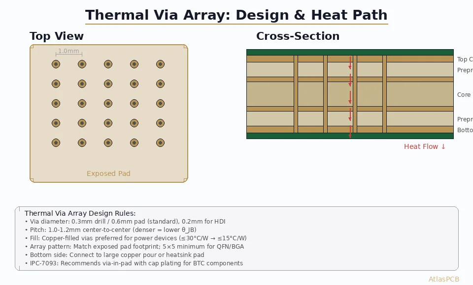
Thermal vias are plated copper holes connecting component thermal pads to internal copper planes or bottom-side heatsinks, reducing junction-to-board thermal resistance by 50–80%. A typical via array of 5×5 vias (0.3 mm drill, 0.6 mm pitch) under a QFN exposed pad achieves approximately 20–30 °C/W thermal resistance, compared to 80–120 °C/W without vias.
The Thermal Challenge in Modern PCBs
Every electronic component generates heat. As packages shrink and power density increases, removing that heat through the PCB becomes a critical design challenge. FR-4 is an effective electrical insulator — but that same property makes it a poor thermal conductor at just 0.25 W/mK through-thickness.
Thermal vias provide a low-resistance path through the board by substituting copper (385 W/mK) for FR-4 in the vertical direction. This guide covers the engineering behind thermal via design, from basic calculations through advanced optimization techniques.
How Thermal Vias Work
Heat Flow Physics
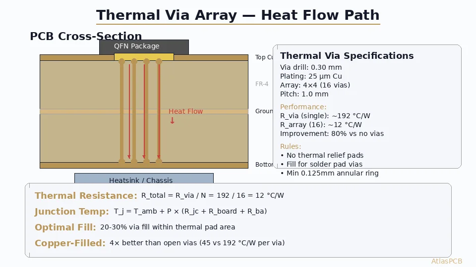
Heat from a component’s thermal pad flows in three paths:
- Lateral spreading through top copper planes (limited by plane area and trace routing)
- Vertical conduction through thermal vias to internal planes and bottom copper
- Convection from exposed copper surfaces to air
Without thermal vias, vertical heat flow is blocked by FR-4 insulation. A 1.6 mm thick FR-4 layer has thermal resistance of approximately 40 °C/W per cm² — making it effectively a thermal insulator in the Z-axis.
Via Thermal Resistance Model
Each plated thermal via can be modeled as a cylindrical copper shell:
R_via = L / (k_Cu × A_annular)
Where:
- L = board thickness (1.6 mm typical)
- k_Cu = copper thermal conductivity (385 W/mK)
- A_annular = π × (r_outer² – r_inner²) = cross-sectional area of copper plating
For a standard via (0.3 mm drill, 25 µm plating):
- r_outer = 0.15 mm
- r_inner = 0.15 – 0.025 = 0.125 mm
- A_annular = π × (0.15² – 0.125²) = 0.0216 mm²
- R_via = 1.6 / (385 × 0.0216 × 10⁻⁶) = 192 °C/W per via
For N vias in parallel: R_total = R_via / N
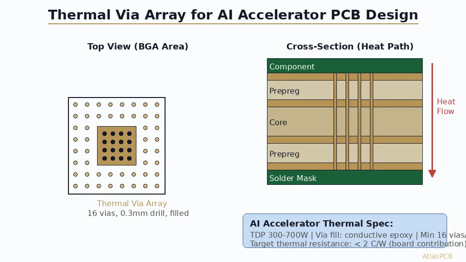
A 4×4 array (16 vias) yields: 192/16 = 12 °C/W — a dramatic improvement.
Filled vs. Plated Vias
| Type | Thermal Resistance per Via | Solderable? | Cost |
|---|---|---|---|
| Open (25 µm plate) | ~192 °C/W | With tenting | Lowest |
| Epoxy-filled + cap plated | ~185 °C/W | Yes | Medium |
| Copper-filled (VIPPO) | ~45 °C/W | Yes | Highest |
| Solid copper rod (press-fit) | ~12 °C/W | N/A | Specialized |
Copper-filled vias are 4× more thermally effective than open vias because the entire cross-section conducts rather than just the barrel plating.
Designing Thermal Via Arrays
Array Sizing for Common Packages
QFN (Quad Flat No-lead) — Exposed Pad
| Pad Size | Recommended Array | Via Drill | Pitch | Estimated R_board |
|---|---|---|---|---|
| 3×3 mm | 3×3 (9 vias) | 0.30 mm | 1.0 mm | 35 °C/W |
| 5×5 mm | 4×4 (16 vias) | 0.30 mm | 1.2 mm | 20 °C/W |
| 7×7 mm | 5×5 (25 vias) | 0.30 mm | 1.3 mm | 14 °C/W |
| 9×9 mm | 6×5 (30 vias) | 0.35 mm | 1.4 mm | 10 °C/W |
LED Thermal Pads
High-power LEDs (3–10 W) need aggressive thermal vias:
- 0.25 mm drill at 0.5 mm pitch (tighter than logic ICs)
- Maximum fill percentage within the thermal pad
- Bottom-side copper must connect to heatsink or MCPCB
Power Amplifiers (GaN, LDMOS)
RF power devices can dissipate 10–100 W:
- Copper-filled vias mandatory above 20 W
- Via arrays extend beyond the package footprint (thermal spreading)
- Via pitch: 0.4–0.6 mm with 0.25 mm drill
- Often combined with heavy copper (3–6 oz) internal planes
Pitch and Drill Size Selection
Via pitch is constrained by:
- Annular ring: Minimum 0.125 mm per side → drill + 0.25 mm = pad diameter
- Manufacturing clearance: Minimum 0.2 mm copper-to-copper between adjacent via pads
- Pitch formula: Min pitch = drill + 2 × annular_ring + clearance
For 0.30 mm drill: Min pitch = 0.30 + 0.25 + 0.20 = 0.75 mm
Practical minimum pitches by drill:
| Drill | Min Pad | Min Pitch | Vias per cm² |
|---|---|---|---|
| 0.20 mm | 0.40 mm | 0.60 mm | 278 |
| 0.25 mm | 0.50 mm | 0.70 mm | 204 |
| 0.30 mm | 0.55 mm | 0.75 mm | 178 |
| 0.35 mm | 0.60 mm | 0.80 mm | 156 |
Via Fill Percentage Optimization
The “fill percentage” is the ratio of via copper area to total pad area:
Fill % = (N × π × r²) / A_pad × 100
Where N = number of vias, r = plated via outer radius, A_pad = exposed pad area.
Diminishing returns occur above ~30% fill:
- 10% fill → ~60% thermal improvement vs. no vias
- 20% fill → ~80% improvement
- 30% fill → ~90% improvement
- 40%+ fill → marginal gains, structural concerns (drill-heavy board)
Optimal target: 20–30% via fill within the thermal pad area.
Multi-Layer Thermal Plane Strategy
Internal Plane Spreading
Thermal vias are most effective when connected to continuous internal copper planes that spread heat laterally:
- Connect vias to every available ground/power plane — maximize thermal spreading area
- Plane clearance: Anti-pads around thermal vias should be minimized (0.15 mm clearance vs. standard 0.25 mm) to maximize plane continuity
- Plane copper weight: 2 oz internal planes provide 2× the lateral spreading of 1 oz copper
Bottom-Side Thermal Relief
The bottom-side connection is where heat ultimately exits:
Option A: Large copper pour with exposed copper (no soldermask)
- Area: At least 4× the component thermal pad area
- Soldermask opening allows direct contact with heatsink
- Thermal interface material (TIM) fills the gap
Option B: Thermal pad array for bottom-side reflow
- Solder to a metal-core insert or copper coin
- Requires careful reflow profile management
Option C: Embedded copper coin
- Mill a cavity in the PCB, press-fit a copper slug
- Best thermal performance (approaches bulk copper)
- Expensive: add $5–15 per board
Thermal Management PCB Design Support
AtlasPCB provides thermal simulation review and copper-fill via processing for high-power designs. Heavy copper (3–10 oz) and embedded coin options available.
Request Thermal DFM Review →Thermal Via Design Rules Checklist
Mandatory Rules
- Via drill ≥ 0.2 mm for reliable plating (smaller vias plate inconsistently)
- Minimum 0.125 mm annular ring for Class 2, 0.15 mm for Class 3
- No thermal relief on thermal vias — direct connection to planes (full connection, not spoke pattern)
- Via array must fit within exposed pad with 0.15 mm edge clearance to prevent solder bridging
- Fill or tent vias if they’re under a solder pad (prevents solder wicking/voiding)
Recommended Practices
- Start with component datasheet thermal pad size — that defines your via array boundary
- Use the maximum number of vias that manufacturing allows at 0.75–1.0 mm pitch
- Connect vias to internal planes with direct connections (thermal relief pads defeat the purpose)
- Provide bottom-side copper area ≥2× the component pad for thermal spreading
- For power modules (>5 W): specify copper-filled vias and consider heavy copper planes
Common Mistakes
| Mistake | Impact | Fix |
|---|---|---|
| Thermal relief on via-to-plane | 3–5× higher resistance | Use full connection |
| Vias outside pad boundary | Solder bridges, shorts | Keep within pad – 0.15 mm |
| Too few vias (< 4) | Negligible improvement | Use minimum 3×3 array |
| No bottom copper area | Heat trapped in via barrel | Add ≥100 mm² exposed copper |
| Open vias under BGA | Solder wicking, voids | Fill and cap-plate |
Simulation and Validation
Quick Analytical Check
Before simulation, estimate junction temperature:
T_j = T_ambient + P × (R_jc + R_board + R_ba)
Where:
- R_jc = junction-to-case (from datasheet, typically 1–20 °C/W)
- R_board = via array thermal resistance (calculated above)
- R_ba = board-to-ambient (depends on copper area and airflow, typically 20–60 °C/W)
Example: A 3 W QFN with R_jc = 5 °C/W, 4×4 via array (R_board ≈ 20 °C/W), and 25 cm² copper bottom (R_ba ≈ 35 °C/W):
- T_j = 25 + 3 × (5 + 20 + 35) = 25 + 180 = 205°C — Too hot!
- Solution: Add heatsink, increase airflow, or use copper-filled vias (R_board ≈ 5 °C/W):
- T_j = 25 + 3 × (5 + 5 + 15) = 25 + 75 = 100°C — Acceptable.
FEA Thermal Simulation
For accurate results, use finite-element analysis:
- Mesh the via array with individual via geometry (barrel + fill)
- Include all copper layers with accurate pour patterns
- Model thermal interface to heatsink or enclosure
- Boundary conditions: Ambient temperature + convection coefficient (5–15 W/m²K natural, 25–80 W/m²K forced)
Tools: Ansys Icepak, Mentor Flotherm, Cadence Celsius, Altium PDN Analyzer (thermal mode)
Application Examples
High-Power GaN Amplifier (50 W)
- Package: GaN HEMT on 4×4 mm thermal pad
- Via array: 7×7 = 49 copper-filled vias, 0.25 mm drill, 0.5 mm pitch
- Board: 6-layer, 3 oz internal planes, 2 oz outer
- Bottom: Exposed copper pad soldered to aluminum heatsink
- Result: R_board < 3 °C/W; T_j = 85°C at full power with forced air
Automotive LED Module (10 W total, 4 LEDs)
- Each LED: 2.5 W on 3×3 mm pad
- Via array per LED: 4×4 = 16 vias, 0.3 mm drill, 0.7 mm pitch
- Board: 4-layer, 2 oz copper, IMS (insulated metal substrate) bottom
- Bottom: Direct thermal path to aluminum housing
- Result: T_j < 95°C for 50,000-hour LED lifetime at 85°C ambient
Data Center ASIC (250 W)
- Package: 45×45 mm LGA with large thermal lid
- Via array: Not primary path (lidded package uses top-side heatsink)
- Thermal vias used for: power delivery plane thermal coupling
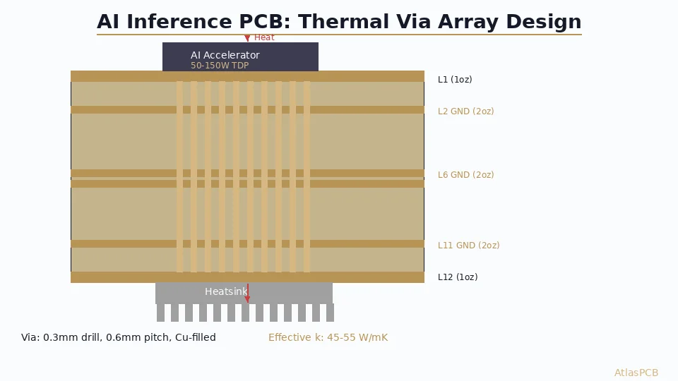
- Supplemental: 8×8 via array connecting bottom power planes to top-side copper reinforcement
- Board: 16-layer HDI, 1 oz copper, liquid cooling on top
Internal Links
- Learn about heavy copper PCB design for maximum current and thermal capacity
- Explore via-in-pad (VIPPO) technology for filled thermal vias under fine-pitch components
- See our PCB stackup design guide for multi-layer thermal plane planning
- Check signal integrity considerations when routing high-speed signals near thermal via arrays
Need help optimizing thermal via arrays for your power design? Get a free DFM review — our engineers will check your via array sizing, copper fill feasibility, and recommend the most cost-effective thermal solution.
About AtlasPCB — We specialize in complex PCB manufacturing for HDI, RF, and high-reliability applications. Explore our aluminum and metal-core PCB services . Every order includes free engineering review. Get your quote.
Reviewed by AtlasPCB Engineering Team — IPC-certified manufacturing specialists with 15+ years of production experience in HDI, RF, and high-reliability PCB fabrication. Content based on factory floor data and real customer design reviews.
Frequently Asked Questions
How many thermal vias do I need under a QFN pad?
Should thermal vias be filled or open?
What is the thermal conductivity of a plated via?
- thermal via
- heat dissipation
- PCB thermal management
- via array
- copper fill
- thermal resistance
- power components