· Marcus Lin · Engineering · 11 min read
Automotive LiDAR PCB Design: Rogers Material Selection and HDI Requirements for ADAS Modules
A technical guide to PCB design and manufacturing for automotive LiDAR modules. Covers Rogers material selection for 905nm/1550nm driver circuits, HDI stackup requirements for TIA and ADC arrays, thermal management for VCSEL drivers, and the AEC-Q100 qualification considerations that affect PCB specification.
Quick Answer
Automotive LiDAR PCBs require hybrid Rogers/high-Tg FR-4 stackups with HDI construction. The RF driver layers (VCSEL/laser driver at 905nm or 1550nm) need Rogers RO4350B or equivalent for controlled impedance at GHz-range pulse frequencies, while the TIA and ADC digital sections use high-Tg FR-4 with HDI microvias for BGA fanout. Typical specification: 8-12 layers, 1+N+1 or 2+N+2 HDI, +/-5% impedance on RF layers, AEC-Q100 Grade 1 compatible (-40 to +125C).
Quick Specification Summary: LiDAR Module PCB
| Parameter | Typical Requirement | Notes |
|---|---|---|
| Layer count | 8-12 | Hybrid stackup |
| RF layers | Rogers RO4350B (1-2 layers) | Driver + antenna feed |
| Digital layers | High-Tg FR-4 (Tg170-180C) | TIA, ADC, FPGA/SoC |
| HDI level | 1+N+1 or 2+N+2 | BGA fanout |
| Min trace/space | 75um/75um (3/3 mil) | HDI layers |
| Impedance tolerance | +/-5% RF, +/-10% digital | Per-layer specification |
| Via-in-pad | Required (TIA, ADC BGAs) | Planarized, copper-filled |
| Temperature range | -40C to +125C | AEC-Q100 Grade 1 |
| Qualification | 1000+ thermal cycles | -40/+125C, 15 min dwell |
| Surface finish | ENIG (typical) | Fine-pitch BGA compatible |
Why LiDAR Pushes PCB Complexity Higher Than Most Automotive
Automotive LiDAR represents a convergence of requirements that few other automotive subsystems demand simultaneously: RF-grade signal integrity for the laser driver, ultra-low-noise analog for the receiver chain, high-density digital for the processing backend, and aggressive thermal management in a compact module that must survive 15 years of automotive environmental exposure.
Most automotive PCBs — even complex ones like ADAS camera modules or radar front-ends — prioritize one or two of these dimensions. A 77 GHz radar board needs RF materials but has relatively simple digital backend. An ADAS processor board needs HDI for large BGA packages but doesn’t require RF-grade dielectrics. LiDAR modules need it all, making them among the most technically demanding PCBs in automotive production.
From our production experience across several Tier 1 LiDAR programs, the dominant challenge isn’t any single parameter — it’s managing the interactions between competing requirements. The thermal cycling requirement limits material choices (no standard FR-4, must use Tg170+ or ceramic-filled). The EMI isolation requirement between driver and receiver sections demands via fencing that consumes routing area. The HDI density requirement creates thin dielectric layers that complicate impedance control on the RF planes. Every design decision cascades into constraints on other parameters.
AUTOMOTIVE RF + HDI
Hybrid Rogers/FR-4 HDI for Automotive Sensor Modules
Impedance-controlled Rogers layers plus HDI digital sections — built to automotive reliability standards. From prototype through PPAP qualification.
Request Quote ›
Material Selection: Why Rogers on the Driver Layer
The Signal Integrity Case for Rogers in LiDAR
A LiDAR transmitter pulses a laser diode (VCSEL array for flash LiDAR, or edge-emitting laser for scanning systems) with rise times typically in the 200ps-1ns range. This creates frequency content extending from DC to 2-5 GHz, depending on the specific pulse shape and modulation scheme. The driver circuit must deliver clean current pulses — typically 2-10A peak for a VCSEL array — through controlled-impedance transmission lines from the driver IC to the laser.
On standard FR-4, two problems emerge at these edge rates. First, the dissipation factor (Df) at 3-5 GHz is approximately 0.018-0.025 for standard FR-4, causing measurable pulse droop and ringing on the current waveform. For a 5cm driver-to-laser trace, this can degrade the pulse leading edge by 10-15% — which directly translates to reduced ranging precision. Second, the Dk variation of +/-10% in FR-4 means your impedance-matched driver network isn’t actually matched, creating reflections that appear as post-pulse oscillation (afterpulsing artifacts in the return signal).
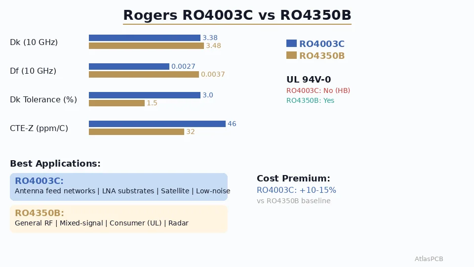
Rogers RO4350B addresses both issues: Df of 0.0037 at 10 GHz means negligible pulse distortion, and Dk tolerance of +/-1.5% ensures the transmission line impedance is predictable. The trade-off is cost (3-5x material premium) and the complexity of hybrid construction — but for automotive LiDAR where ranging accuracy specifications leave no margin, the engineering case is clear.
Material Selection for Different LiDAR Wavelengths
The choice between 905nm and 1550nm LiDAR systems doesn’t directly change PCB material requirements (since the PCB carries the electrical driver signal, not the optical wavelength), but it does affect thermal requirements. 1550nm systems typically use InGaAs photodetectors that require less cooling, while 905nm VCSEL arrays generate more waste heat at higher drive currents. This thermal consideration affects copper weight selection and thermal via density on the driver section — which in turn affects stackup thickness and impedance calculations.
HDI Architecture: Fanout for Modern LiDAR SoCs
Why Standard Through-Hole Won’t Work
Modern LiDAR receiver front-ends integrate the TIA array, ADC, and digital processing into a single SoC or multi-chip package. These devices typically use flip-chip BGA packages with 0.5mm or 0.65mm ball pitch and 200-400 balls. At 0.5mm pitch, the BGA pad diameter is approximately 0.25mm with 0.25mm gap between pads — making it physically impossible to route escape traces between pads using standard mechanical drills (minimum 0.15mm drill produces 0.3mm finished hole plus 0.5mm pad).
The solution is HDI construction with laser-drilled microvias: 75um laser vias with 200-250um capture pads enable via-in-pad fanout directly from the BGA balls. A 1+N+1 structure (one buildup layer on each side) handles most 0.65mm-pitch BGAs, while 0.5mm pitch typically requires 2+N+2 for full breakout of central balls.
Stackup Architecture
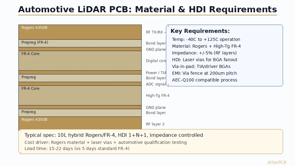
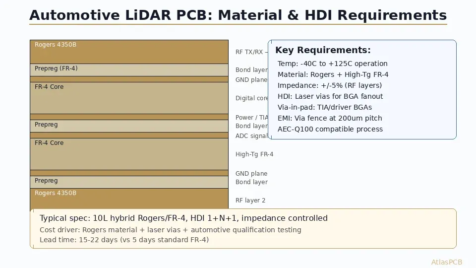
A representative 10-layer LiDAR module stackup:
Layer 1: Rogers RO4350B — VCSEL driver traces (50-ohm controlled impedance) Layer 2: Ground plane (continuous, RF reference) Layer 3: High-Tg FR-4 — TIA analog signals (differential pairs, controlled impedance) Layer 4: Ground plane (analog/digital boundary) Layer 5: High-Tg FR-4 — ADC digital routing Layer 6: Power plane (segmented: analog VDD, digital VDD, laser VDD) Layer 7: High-Tg FR-4 — Digital routing (SPI, LVDS, clock) Layer 8: Ground plane (digital reference) Layer 9: High-Tg FR-4 — Power distribution, decoupling Layer 10: Rogers RO4350B — Secondary RF / calibration circuits
The HDI buildup adds Layer 1 (buildup with microvia to L2) and Layer 10 (buildup with microvia to L9), making this a 1+8+1 construction. The Rogers layers are placed on the outermost core positions for manufacturing simplicity — they can be pressed as standard cores before the HDI buildup is applied.
HDI MANUFACTURING
Up to 5+N+5 HDI with Via-in-Pad and Stacked Microvias
Laser-drilled microvias down to 75um, copper-filled and planarized. Sequential lamination for any-layer interconnect on automotive-grade substrates.
Thermal Management: VCSEL Driver Heat Dissipation
Automotive LiDAR modules generate significant heat in a compact area. A typical flash LiDAR VCSEL array dissipates 5-15W peak during emission pulses (duty cycle typically 0.1-1%), with average dissipation of 1-3W. The driver IC itself may dissipate an additional 2-5W continuously. Combined with the digital processing backend (3-10W for a LiDAR SoC), total module dissipation can reach 15-20W in a package the size of a credit card.
The PCB’s role in thermal management is critical. Thermal vias under power components (via arrays with 0.3mm diameter, 0.6mm pitch) conduct heat from the component side to internal ground planes that act as heat spreaders. For the VCSEL driver section, we typically recommend a dedicated thermal ground plane with direct via connection to an external heat sink mounting area. Copper weight on power planes should be 2oz minimum (preferably 3oz) for effective lateral heat spreading.
One challenge specific to hybrid Rogers/FR-4 boards: Rogers RO4350B has lower thermal conductivity (0.69 W/mK) than FR-4 (approximately 0.3 W/mK through-plane, 0.8 W/mK in-plane for standard glass-reinforced). This means the Rogers layers actually perform slightly better for in-plane heat spreading than through-plane conduction. Design thermal via arrays to bypass the Rogers layers and conduct heat directly through the copper planes.
EMI Isolation: Via Fencing Between Driver and Receiver
The critical EMI challenge in LiDAR PCB design is preventing the high-current driver pulses (2-10A at nanosecond edges) from coupling into the ultra-sensitive TIA receiver input (which must detect return signals in the nanoamp to microamp range — a dynamic range of 60-80 dB below the driver signal).
PCB-level isolation uses three mechanisms:
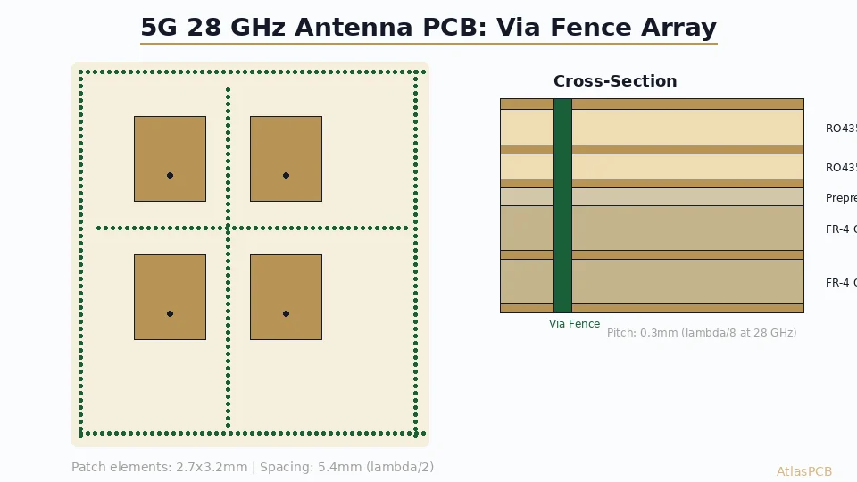
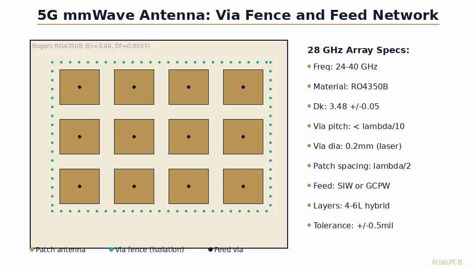
Via fencing (ground via walls): A complete wall of ground vias between the driver and receiver sections, spaced at lambda/4 at the highest frequency of concern. For a 5 GHz maximum frequency (covering driver switching harmonics), this translates to approximately 3mm pitch in FR-4, or 4mm pitch in Rogers. Our recommendation for automotive LiDAR: 200um-pitch laser vias forming a continuous stitched wall — this provides 40+ dB of isolation at 5 GHz based on our test coupon measurements.
Split ground planes: Separate ground planes for driver and receiver sections, connected at a single point near the power entry. This prevents return current from the driver flowing through the receiver ground reference. The connection point should include a ferrite bead for high-frequency isolation.
Physical separation: Minimum 5mm clearance between driver output traces and TIA input traces, with ground fill in between. For boards where space doesn’t permit 5mm clearance, increase via fence density to compensate.
AEC-Q100 Qualification: What It Means for PCB Specification
AEC-Q100 is technically a component qualification standard (for ICs), but automotive Tier 1 suppliers extend its environmental requirements to the PCB as a component of the module. The relevant parameters for PCB specification:
Grade 1 temperature range (-40C to +125C): Requires high-Tg FR-4 (Tg170C minimum, preferably Tg180C) and validation that the Rogers/FR-4 hybrid bond survives thermal cycling across this range. CTE mismatch between Rogers Z-axis (32 ppm/C) and FR-4 Z-axis (50-70 ppm/C) creates stress at the boundary — manageable with proper prepreg selection but must be validated by thermal cycling test.
1000-cycle thermal shock: The PCB must survive 1000 cycles of -40C to +125C (15-minute dwell, air-to-air transfer) with no delamination, barrel cracking, or impedance shift greater than specified tolerance. We’ve found that hybrid Rogers/FR-4 boards require careful attention to the bonding prepreg to pass this test consistently — standard 1080 prepreg is marginal; 2116 or thicker glass styles perform better at the material boundary.
Moisture sensitivity (MSL): While MSL is primarily a component concern, PCBs destined for automotive applications should be baked (125C, 24h) before assembly if stored more than 72 hours after manufacture, to prevent moisture-induced delamination during reflow.
AUTOMOTIVE GRADE
Thermal Cycling Qualified, Rogers + HDI, IATF 16949 Process
From design review through PPAP. We support automotive Tier 1 programs with engineering-grade hybrid PCBs that survive -40C to +125C for 1000+ cycles.
Start Automotive Project ›Manufacturing Considerations: Lead Time and Complexity
Automotive LiDAR boards are among the most complex PCBs to manufacture. The combination of hybrid materials, HDI, tight impedance, and automotive-grade inspection means lead times are typically 15-22 working days for prototype quantities — compared to 5-7 days for a standard 8-layer FR-4 board.
Key manufacturing steps that add time: Rogers material procurement (2-3 days if not in stock), sequential lamination for HDI buildup (additional press cycle per side), laser drilling with precise depth control, copper fill and planarization of via-in-pad structures, and comprehensive impedance testing on every panel. The automotive inspection requirements (100% AOI both sides, microsection per lot, impedance test every panel) add additional processing time.
For production programs, we recommend establishing a material allocation agreement: pre-purchasing Rogers material for 3-6 months of production eliminates the longest lead-time component and locks in pricing. Most Rogers distributors offer blanket order programs for automotive-volume quantities.
Summary: Specification Checklist for LiDAR Module PCB
When preparing a LiDAR module PCB specification for quotation, ensure these elements are defined:
- Complete stackup with material callouts per layer (Rogers P/N, FR-4 grade, prepreg style)
- Impedance targets per layer with tolerance specification
- HDI structure type (1+N+1, 2+N+2) with via sizes and pad dimensions
- Thermal via array specifications (pitch, diameter, plating thickness)
- Via fence specifications (pitch, connectivity, layer span)
- Temperature range and thermal cycling requirement (cycles, dwell time)
- Surface finish with BGA compatibility requirement
- Qualification test plan (thermal cycling, hi-pot, microsection criteria)
- Panel quantity and delivery schedule
- Documentation requirements (CoC, test data, material certs)
Missing any of these will result in either an incomplete quote or manufacturing assumptions that may not match your design intent.
ATLASPCB
Building a LiDAR or Automotive Sensor Module?
Upload your design for engineering review. We'll verify stackup feasibility, provide DFM feedback on your HDI and RF layers, and quote prototype through production quantities with automotive-grade quality.
Upload LiDAR Design ›
Reviewed by AtlasPCB Engineering Team — 15+ years in advanced PCB fabrication for RF, HDI, and rigid-flex applications.
Related Reading:
About AtlasPCB — We specialize in complex PCB manufacturing for HDI, RF, and high-reliability applications. Explore our HDI PCB manufacturing capabilities, RF and high-frequency PCB services, or get an Rogers RO4350B PCB manufacturing . Every order includes free engineering review. Get your quote.
Reviewed by AtlasPCB Engineering Team — IPC-certified manufacturing specialists with 15+ years of production experience in HDI, RF, and high-reliability PCB fabrication. Content based on factory floor data and real customer design reviews.
Frequently Asked Questions
Why does an automotive LiDAR PCB need Rogers material?
What HDI level is typical for LiDAR sensor boards?
What temperature range must an automotive LiDAR PCB survive?
How does EMI shielding work on a LiDAR PCB?
What is the typical cost for an automotive LiDAR PCB?
- Rogers PCB manufacturer
- HDI PCB manufacturer
- PCB manufacturer for aerospace
- RF PCB design and manufacturing
- Rogers 4350B stackup