· David Okafor · Engineering · 10 min read
China PCB Prototype vs Production: When Budget Fabs Hit Their Limits
A practical guide for hardware engineers on when to switch from budget Chinese prototype fabs (JLCPCB, PCBWay) to engineering-grade manufacturers. Covers the technical triggers, cost crossovers, and qualification gaps that signal it's time to move up.
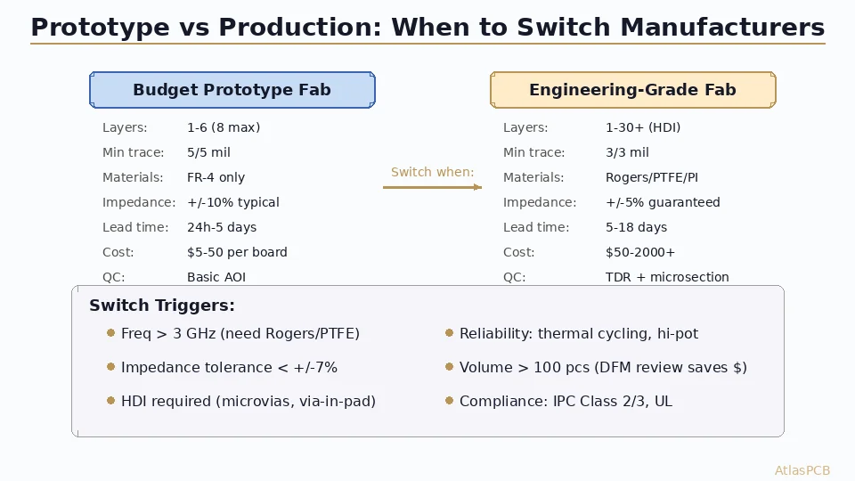
Quick Answer
Switch from a budget prototype fab to an engineering-grade manufacturer when your design requires impedance tolerance below +/-7%, RF materials (Rogers/PTFE), HDI construction, or reliability testing beyond basic electrical test. The cost premium of 3-8x per board pays for itself when you factor in respins, qualification failures, and field returns that budget fabs cannot prevent.
30-Second Decision: Should You Switch?
| Your Situation | Stay on Budget Fab | Switch to Engineering-Grade |
|---|---|---|
| 2-4L FR-4, digital only | Yes | No |
| Impedance +/-10% OK | Yes | No |
| Frequency < 1 GHz | Yes | No |
| RF > 2 GHz, need Rogers | No | Yes |
| HDI (microvias, via-in-pad) | No | Yes |
| Impedance +/-5% required | No | Yes |
| IPC Class 3 / automotive | No | Yes |
| Volume > 100 pcs, complex | No | Yes |
Why This Decision Matters More Than You Think
Every hardware startup and engineering team goes through the same arc: prototype on JLCPCB or PCBWay because it’s fast and cheap, get the design working on the bench, then move to “real production.” The problem is that many teams make this transition too late — after a qualification failure, a field return, or a mysterious RF performance gap between their prototype and the next build.
The budget Chinese prototype fabs have revolutionized hardware development. A 4-layer board in 48 hours for $15 is genuinely remarkable, and for a huge class of designs, that’s all you’ll ever need. But these services optimize for exactly one thing: getting you a board that looks correct as fast as possible. They do not optimize for process control, material consistency, or parametric performance — because their pricing model cannot support it.
In our facility, we process roughly 200 orders per month that are “migrations” from budget prototype fabs — engineers who discovered their prototype worked but their pre-production batch didn’t meet spec. The most common pattern: a 4-layer impedance-controlled board that happened to measure within spec on the JLCPCB prototype (because their process landed in the right window that day), but then fails on the second build because the process window shifted. The engineer blames their redesign, but the root cause was never having controlled impedance in the first place.
RF & HIGH-SPEED DESIGNS
Need Tighter Specs Than Your Prototype Fab Can Deliver?
Upload your Gerbers for a free manufacturability assessment. We'll tell you exactly where budget fab limits will bite you.
Upload Gerbers ›
The Technical Triggers: When Budget Fabs Cannot Deliver
RF Materials (Rogers, PTFE, Polyimide)
This is the clearest trigger. Budget fabs run FR-4 exclusively — they don’t stock Rogers RO4350B, RO4003C, or any PTFE laminate, and they don’t have the press profiles calibrated for these materials. If your design operates above 2-3 GHz and needs controlled dielectric properties, you physically cannot have it made at a budget prototype house.
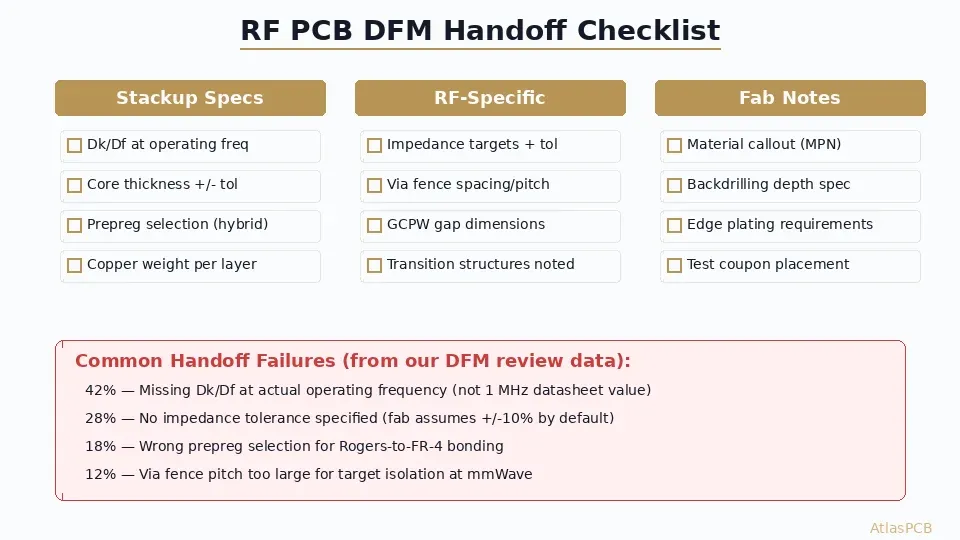
The more subtle version: your design uses FR-4 at 2.4 GHz WiFi and “works,” but you’re seeing 2-3 dB more insertion loss than your simulation predicted. That’s because budget fab FR-4 has Dk variation of +/-10-15% batch-to-batch, and Df that can range from 0.018 to 0.025 depending on the resin system they happened to use that week. At 2.4 GHz, that variation is measurable. At 5.8 GHz, it’s significant. At 24+ GHz, the board is unusable.
Impedance Control Below +/-7%
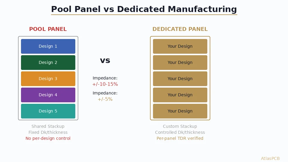
Budget fabs advertise “impedance control” but the reality is different from what most engineers expect. Their process involves running your stackup through a field solver, adjusting trace widths, and then manufacturing the board on whatever panel happens to be in the queue. They rarely measure the actual Dk of the incoming laminate lot, they don’t run test coupons on every panel, and their TDR measurement (if performed at all) is a spot-check on one coupon per production lot — not per panel, certainly not per board.
In our experience processing boards that “failed impedance” after being prototyped at budget fabs, the actual impedance scatter is typically +/-12-15% for single-ended 50-ohm traces on their standard stackups. They hit +/-10% most of the time because their nominal process is centered reasonably well, but the tails are wide. For applications requiring +/-5% or tighter — DDR4/5 routing, USB3/4, PCIe Gen4+, or any RF matching network — budget fabs cannot guarantee the result.
HDI Construction
High Density Interconnect is where budget fabs fall hardest. True HDI requires laser drilling (UV or CO2), sequential lamination, and precise registration between buildup layers. Budget fabs offer mechanical drilling down to 0.2mm and standard lamination — they may advertise “blind vias” but these are typically achieved through controlled-depth mechanical drilling, not laser processing. The result has larger pad sizes, worse aspect ratios, and cannot achieve via-in-pad with reliable copper fill.
If your design requires 0.4mm-pitch BGA fanout, stacked microvias, or any-layer interconnect, budget fabs simply cannot build it. Even their “HDI” offerings (which some now advertise) are limited to 1+N+1 configurations with relatively large laser vias (100-125um) and no stacking.
The Cost Reality: When “Cheap” Becomes Expensive
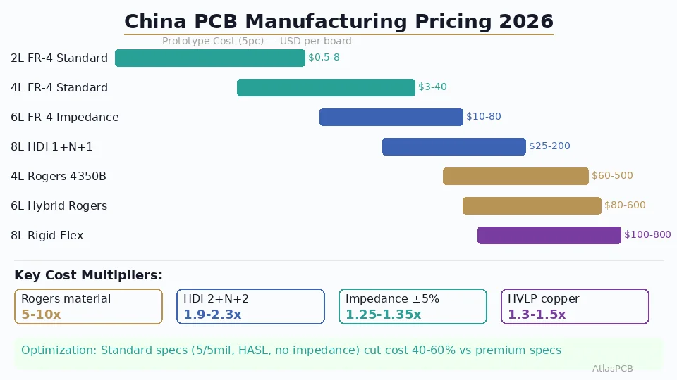
The most common objection to switching manufacturers is cost. And at prototype quantities, the math does favor budget fabs — $15 for 5 boards versus $200-500 for the same quantity at an engineering-grade facility. But this comparison misses three hidden costs that flip the equation:
Respin cost: When a budget-fab prototype “works” but production boards don’t, you’ve wasted 4-8 weeks and $2,000-10,000 in engineering time debugging a manufacturing issue masquerading as a design problem. We see this approximately 15-20 times per month in orders that come to us after a failed production attempt elsewhere.
Qualification failure cost: For medical, automotive, or aerospace applications, boards that pass bench testing but fail environmental qualification (thermal cycling, vibration, humidity) because the manufacturing process wasn’t controlled tightly enough. A qualification failure can cost $50,000-200,000 in retest fees, schedule delays, and lost customer confidence.
Field return cost: The most expensive scenario. Boards that ship to customers and fail in the field due to marginal manufacturing — intermittent connections from poorly filled vias, impedance-related signal integrity issues that only appear at temperature extremes, or delamination from incompatible prepreg. One field failure in a medical or automotive product can cost more than the entire production run.
COMPARE YOUR OPTIONS
Get a Quote to Compare Against Your Current Fab
See exactly what engineering-grade manufacturing costs for your specific design. No surprises at production time.
Get Instant Quote ›The Volume Crossover Point
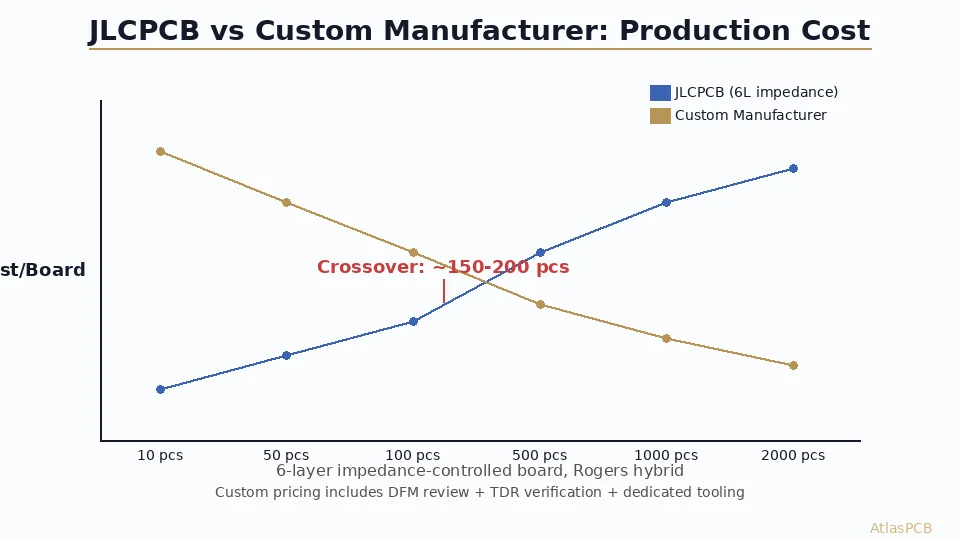
At very low volumes (5-10 boards), budget fabs win on unit cost for simple designs. But as volume increases, the math changes because engineering-grade fabs offer:
Panel optimization: At 50+ boards, a proper manufacturer optimizes panel utilization, sometimes reducing per-board cost by 20-30% compared to the standard 100x100mm panel assumption. Budget fabs use fixed panelization — your boards get whatever standard array they use.
Yield guarantee: Engineering-grade fabs typically guarantee 98-99%+ yield for boards built within their documented capability. Budget fabs have no yield guarantee, and at 100+ boards, their 5-15% scrap rate on complex designs means you’re paying for boards you never receive.
DFM optimization: A proper engineering review before production can identify cost-saving opportunities — slightly widening a trace, adjusting a via size, or modifying a copper balance layer — that reduce production cost by 10-20% without affecting performance. Budget fabs build exactly what you send, even if minor changes would improve yield and reduce cost.
For most complex designs (6+ layers, impedance controlled, any RF or HDI), the practical crossover is around 50-100 boards. Below that, the engineering-grade premium is pure quality insurance. Above that, the better yield, DFM optimization, and process control start closing the unit cost gap.
How to Transition Without Losing Time
The transition from budget to engineering-grade manufacturing doesn’t have to be disruptive. Here’s the process we recommend based on handling hundreds of these migrations:
Step 1: Design audit. Send your Gerbers and stackup for a DFM review before committing to a build. An engineering-grade fab will identify potential issues that your budget prototype happened to survive but that won’t survive at tighter process control. Common findings: trace widths need adjustment for target impedance on the actual laminate Dk, via aspect ratios need modification for reliable plating, and copper balance layers need optimization.
Step 2: First article with full verification. Run a small quantity (5-10 boards) with full TDR impedance verification, microsection at critical vias, and impedance/loss measurement at your operating frequency. This establishes the manufacturing baseline and confirms your simulation models.
Step 3: Production release. With the first article approved, production runs follow the same process recipe with ongoing SPC monitoring. Test coupons on every panel ensure each board meets spec, not just the first article.
ENGINEERING-GRADE FABRICATION
Rogers, HDI, Impedance Controlled — Built Right the First Time
TDR-verified impedance, microsection QA, full material traceability. From prototype through production.
What to Look For in an Engineering-Grade Chinese Manufacturer
Not all “custom” PCB manufacturers are equal. When evaluating options beyond budget fabs, verify these capabilities:
Material handling: Do they stock Rogers, Taconic, and PTFE materials? Can they provide material certificates for each lot? Hybrid Rogers/FR-4 builds require specific press profiles and bonding materials — ask about their experience with mixed-material lamination.
Process control documentation: Can they provide Cpk data for their drilling, plating, and etching processes? Engineering-grade facilities track process capability indices and adjust tooling before tolerance drift becomes yield loss.
Testing capabilities: TDR impedance measurement (not just calculated from stack), 4-wire Kelvin resistance testing, ionic contamination measurement, microsection analysis in-house. If they outsource testing, turnaround is slow and issues aren’t caught during production.
Qualification support: For automotive (IATF 16949), medical (ISO 13485), or aerospace (AS9100) applications, the fab should either hold relevant certifications or demonstrate equivalent process control with documented procedures.
Summary: The Decision Framework
The choice between budget and engineering-grade PCB manufacturing isn’t about “good vs bad” — it’s about matching your fab’s capabilities to your design’s requirements. Use budget fabs for what they excel at: fast, cheap prototypes of simple boards. Use engineering-grade manufacturers when your design demands precision that budget processes cannot deliver.
The expensive mistake isn’t paying more per board — it’s discovering at qualification or in the field that your “working prototype” was working by accident, not by design.
ATLASPCB
Ready to Move Beyond Budget Prototyping?
Upload your design for a detailed manufacturability assessment. We'll identify specs that need engineering-grade process control — and quote both prototype and production quantities.
Upload Design ›
Reviewed by AtlasPCB Engineering Team — 15+ years in advanced PCB fabrication for RF, HDI, and rigid-flex applications.
Related Reading:
About AtlasPCB — We specialize in complex PCB manufacturing for HDI, RF, and high-reliability applications. Explore our HDI PCB manufacturing capabilities, RF and high-frequency PCB services, or get an impedance-controlled PCB manufacturing . Every order includes free engineering review. Get your quote.
Reviewed by AtlasPCB Engineering Team — IPC-certified manufacturing specialists with 15+ years of production experience in HDI, RF, and high-reliability PCB fabrication. Content based on factory floor data and real customer design reviews.
Frequently Asked Questions
When should I stop using JLCPCB or PCBWay for my projects?
How much more expensive is a custom PCB manufacturer vs JLCPCB?
Can I prototype on a budget fab and then move to production elsewhere?
What technical capabilities do budget fabs typically lack?
Is there a volume crossover where budget fabs become worse value?
- JLCPCB vs custom PCB manufacturer
- China RF PCB manufacturer
- PCB prototype
- impedance controlled PCB manufacturer
- HDI PCB manufacturer