· AtlasPCB Engineering · Engineering · 9 min read
HDI PCB Cost Breakdown: Microvia Stacks, Layer Count, and Pricing Optimization (2026)
What drives HDI PCB cost? Detailed pricing analysis of sequential lamination, microvia types, layer counts from 6 to 24 layers, and practical optimization strategies that reduce cost 20-40% without sacrificing routing density.
Quick Answer
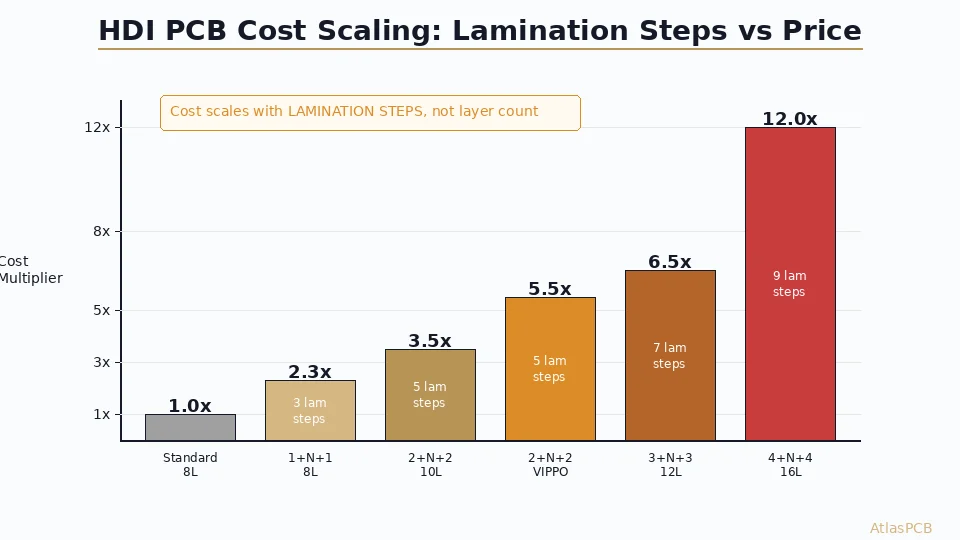
HDI PCB cost is driven primarily by sequential lamination steps (each adds 30-50% to base cost), microvia type (stacked vias cost 2-3x more than staggered), and total layer count. A 6-layer 1+N+1 HDI board costs approximately 2-2.5x a standard 6-layer, while a 12-layer 3+N+3 with stacked microvias costs 5-8x the standard equivalent. Key optimization: reduce sequential lamination steps, use staggered instead of stacked microvias where routing allows, and minimize aspect ratios.
Quick Answer: HDI Cost Scaling
| HDI Structure | Lamination Steps | Cost vs Standard ML | Typical Use Case |
|---|---|---|---|
| Standard 8L (TH only) | 1 | 1x (baseline) | General digital, < 0.8mm pitch BGA |
| 1+N+1 (8L) | 3 | 2.0-2.5x | 0.5-0.65mm pitch BGA breakout |
| 2+N+2 (10L) | 5 | 3.0-4.0x | 0.4-0.5mm pitch BGA, fine-pitch mobile |
| 3+N+3 (12L) | 7 | 5.0-8.0x | 0.35-0.4mm pitch, FPGA/SoC |
| Any Layer (ELIC) | 2N+1 | 8-15x | Ultra-fine pitch, < 0.3mm, chip-scale |
The cost multiplier is not layer count — it is lamination count. A standard 12-layer board has 1 lamination step. A 12-layer 3+N+3 HDI has 7. That processing multiplication is the primary cost driver.
What Actually Costs Money in HDI Fabrication
HDI cost is misunderstood. Engineers often assume that laser drills and microvias are what make HDI expensive. In reality, the laser drilling itself is fast and relatively cheap per hole. What makes HDI expensive is the number of sequential processing passes required — each of which is essentially fabricating a complete board with its own imaging, plating, etching, and inspection cycle.
To understand why, consider how a 2+N+2 HDI board is fabricated. The manufacturer starts by building the core layers (N) as a standard multilayer PCB — that is one complete fabrication cycle. Then they laminate the first buildup layer on each side, laser drill microvias, plate them, image the pattern, and etch. That is fabrication cycle two. Then they laminate the second buildup layer on each side and repeat: laser drill, plate, image, etch — cycle three. Each cycle takes the same time, uses the same equipment, requires the same quality inspection, and carries its own yield risk.
In our production, a 4-layer standard PCB takes 5 days through fabrication. A 10-layer 2+N+2 HDI takes 14-18 days — not because individual steps are slower, but because there are three times as many of them, and each must complete fully before the next begins. This sequential nature is fundamentally what drives cost. Parallel processing (like multiple panels in the same etch bath) helps throughput but not lead time.
The yield compound effect is equally important. If each lamination cycle has a 95% yield (which is good), a 1-lamination standard board yields 95% good panels. A 3-step HDI yields 0.95 x 0.95 x 0.95 = 85.7%. A 5-step yields 77.4%. Each step multiplies by the yield factor, and the cost per good board must account for the panels lost at each stage. This is why HDI pricing does not scale linearly with layer count — it scales exponentially with lamination count.
HDI PCB MANUFACTURER
Get an Accurate HDI Quote — Not a Guess
Upload your design and we will quote based on actual layer structure, microvia type, and panel utilization. No hidden upcharges for HDI — the price reflects real fabrication complexity.
Get HDI Quote ›
Microvia Type: Stacked vs Staggered Cost Impact
The choice between stacked and staggered microvias has a 2-3x cost impact that many designers do not realize until quoting. Both achieve layer-to-layer connection through buildup layers, but the fabrication requirements differ significantly.
Staggered microvias offset the position of each layer’s via relative to the layer below. The via on layer 1-2 lands on a pad, and the via from layer 2-3 starts at a different X-Y location on that same pad. This works because the landing pad is large enough to capture both via positions (typically 350-400 um pad for 100 um via). The advantage: each microvia can be standard laser-drilled and copper-plated without requiring complete copper fill. Standard electrolytic plating that fills the via 60-80% is sufficient because the next via starts at a different position.
Stacked microvias place each layer’s via directly on top of the previous layer’s via. This requires the lower via to be completely filled with copper and planarized flat (the VIPPO process — Via In Pad Plated Over) so the next via has a solid copper target to land on. The filling and planarization adds a processing step at every lamination cycle: plate fill, mechanical or chemical planarization, then proceed to next lamination. This step alone adds 15-25% to the processing time per cycle.
From our production data, the cost breakdown between the two approaches on a 10-layer 2+N+2 design (100x100mm, qty 50 pieces):
| Configuration | Per-Board Cost | Key Cost Delta |
|---|---|---|
| 2+N+2 staggered microvias | $38-52 | Baseline HDI |
| 2+N+2 stacked microvias (VIPPO) | $65-95 | +70-85% for fill/planarize |
The engineering tradeoff: stacked vias save routing space (smaller landing pads since the via stack occupies a single X-Y location) and are sometimes required for ultra-fine-pitch BGAs below 0.4mm where pad geometry does not allow stagger offset. For 0.5mm pitch and above, staggered microvias almost always provide sufficient routing space at significantly lower cost.
Layer Count Optimization: When More Layers Cost Less
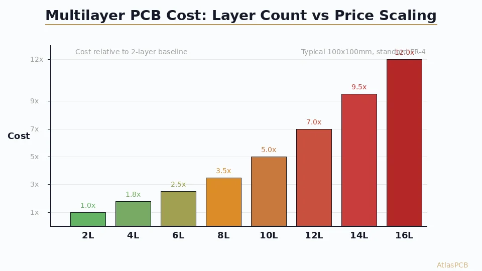
Counter-intuitively, adding standard through-hole layers to the core can sometimes reduce total cost compared to adding HDI buildup layers. This works because core layers are fabricated in a single lamination step, while each HDI buildup requires its own sequential pass.
Consider two approaches to routing a design that needs 10 routing layers:
Option A: 10-layer 3+N+3 (N=4 core layers)
- 7 lamination steps
- Cost multiplier: ~6x standard 10-layer
- Lead time: 20-25 days
Option B: 14-layer 2+N+2 (N=10 core layers)
- 5 lamination steps
- Cost multiplier: ~3.5x standard 14-layer
- Lead time: 15-18 days
Option B has more total layers but fewer sequential lamination steps. The additional core layers cost comparatively little (standard multilayer process), while the eliminated HDI steps save significant money. The total cost of Option B is often 20-30% lower than Option A, despite having 4 more layers.
This analysis changes at very fine pitch where you genuinely need the routing density that only 75 um trace/space on HDI layers provides. But for designs that need density only in the BGA escape region and have relaxed routing elsewhere, expanding the core and minimizing HDI steps is the most effective cost optimization we recommend.
Our process engineers evaluate this tradeoff for every HDI quote. When a customer submits a 3+N+3 design, we check whether a 2+N+2 with additional core layers achieves the same routing — and if so, we propose the cheaper alternative.
COST OPTIMIZATION
We Propose the Most Cost-Effective HDI Structure
Our engineering team reviews your BGA pitch and routing requirements to recommend minimum-cost HDI configuration — staggered vs stacked, optimal core layer count, and panel utilization.
HDI Capabilities ›Real Pricing Examples (2026 Market Rates)
Based on our current production pricing for commonly ordered HDI configurations (100x100mm board size, standard FR-4 Tg170, ENIG finish, 1 oz copper):
| Configuration | Qty 5 | Qty 50 | Qty 500 | Key Specs |
|---|---|---|---|---|
| 6L standard (TH) | $12-18 | $6-9 | $3-5 | 0.15mm min drill, 4/4mil T/S |
| 6L 1+N+1 HDI | $28-42 | $14-20 | $7-11 | 0.1mm laser via, 3.5/3.5mil T/S |
| 8L 1+N+1 HDI | $35-55 | $18-28 | $9-14 | Single buildup each side |
| 10L 2+N+2 HDI (staggered) | $55-85 | $32-48 | $16-24 | 0.1mm laser via, via-in-pad |
| 10L 2+N+2 HDI (stacked VIPPO) | $90-140 | $52-78 | $28-40 | Filled + planarized vias |
| 12L 3+N+3 HDI (staggered) | $120-180 | $65-95 | $35-52 | Full HDI, high-density escape |
| 16L 4+N+4 HDI (stacked) | $250-400 | $130-200 | $72-110 | Ultra-HDI, any-layer connect |
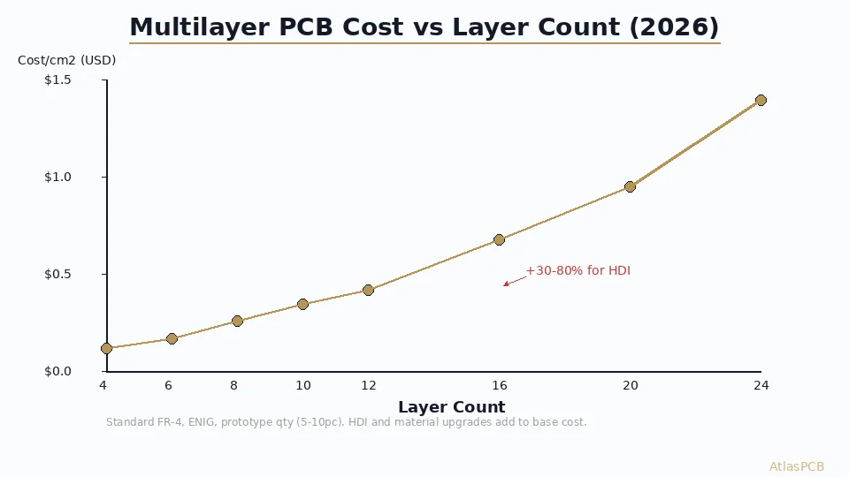
These prices reflect 2026 market conditions with stable laminate supply. Prices increase 20-30% for Rogers core layers, 10-15% for immersion silver or ENEPIG finish, and 10-20% for halogen-free materials. Panel utilization significantly affects per-board cost — boards larger than 250x200mm may not fit standard panels efficiently, adding 15-25% waste factor.
Volume pricing note: The most dramatic cost reduction happens between qty 5 and qty 50 because NRE (laser programs, imaging tooling, test fixtures) amortizes. Between 50 and 500, per-unit cost drops more gradually as panel yield and material purchasing volume improve.
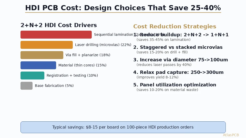
Cost Reduction Checklist for Your Next HDI Design
Before finalizing your HDI stackup, evaluate these optimization opportunities that our engineering team checks on every design review:
First, verify that you actually need HDI. If your finest-pitch BGA is 0.5mm and you have only one such component, you may achieve breakout on a standard board with via-in-pad (which still requires fill-and-plate but avoids sequential lamination entirely). We see approximately 20% of designs submitted as “HDI” that can achieve full routing on standard multilayer with via-in-pad and careful planning.
Second, minimize the maximum HDI depth. If you need 2+N+2 only in one small region under a BGA, consider whether you can route everything else through the core and use HDI microvias only for BGA escape. Some designers request 3+N+3 because one signal needs to transition from L1 to L4 — but that same connection can often route through a dog-bone fanout to a through-hole via, eliminating an entire lamination step.
Third, optimize panel utilization. HDI boards are processed as full panels regardless of your board size. A 50x50mm board puts 4-6 units per panel (high utilization, efficient). A 180x120mm board puts 1-2 units per panel (lower utilization, each unit bears more overhead). If panel utilization is below 50%, consider whether the board outline can be compacted.
ATLASPCB
Get Your HDI Board Quoted Today
Upload your Gerbers and we will quote your HDI design with cost optimization recommendations. Up to 5+N+5 buildup, stacked and staggered microvias, via-in-pad VIPPO.
Upload Design ›
Reviewed by AtlasPCB Engineering Team — 15+ years in advanced PCB fabrication for RF, HDI, and rigid-flex applications.
Related Reading:
About AtlasPCB — We specialize in complex PCB manufacturing for HDI, RF, and high-reliability applications. Explore our HDI PCB manufacturing capabilities, multilayer PCB fabrication up to 30 layers, or get an instant online PCB quote . Every order includes free engineering review. Get your quote.
Reviewed by AtlasPCB Engineering Team — IPC-certified manufacturing specialists with 15+ years of production experience in HDI, RF, and high-reliability PCB fabrication. Content based on factory floor data and real customer design reviews.
Frequently Asked Questions
How much more expensive is HDI vs standard PCB?
What is the biggest cost driver in HDI PCB fabrication?
Are stacked microvias more expensive than staggered?
How do I reduce HDI PCB cost without losing routing density?
What is the minimum quantity for HDI PCB to be cost-effective?
- HDI PCB manufacturer
- multilayer PCB cost
- HDI PCB cost
- PCB stackup design guide
- microvia PCB