· Sophia Reyes · Engineering · 11 min read
How to Specify Impedance Requirements for Your PCB Manufacturer: A Complete DFM Guide
Everything your fab drawing needs to get impedance-controlled PCBs right on the first order. Covers single-ended and differential specs, tolerance bands, coupon requirements, and the common mistakes that cause 60% of impedance failures.
Quick Answer
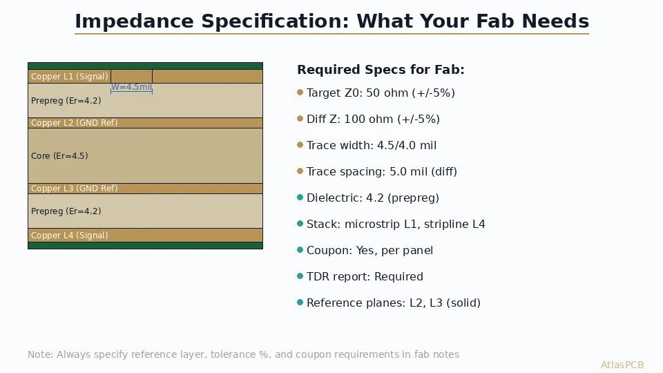
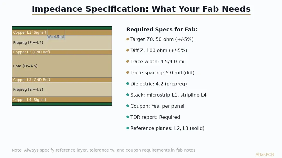
Specify impedance on your PCB by including: target impedance value and tolerance (e.g., 50 ohm +/-10%), reference layer designation, trace width and spacing from your EDA stackup simulation, dielectric constant and thickness assumptions, and whether you require TDR coupon verification. Place this information in your fab drawing notes and stackup table — never assume the manufacturer will calculate it from your Gerbers alone.
Quick Reference: Impedance Specification Checklist
Before submitting your design to any PCB manufacturer, verify these items are documented in your fab drawing:
| Required Information | Example | Where to Specify |
|---|---|---|
| Target impedance (single-ended) | 50 ohm +/-10% | Fab drawing notes |
| Target impedance (differential) | 100 ohm +/-10% | Fab drawing notes |
| Reference layer(s) | L2 ground plane | Stackup table |
| Trace width (calculated) | 4.5 mil | Stackup table |
| Differential pair spacing | 5.0 mil gap | Stackup table |
| Dielectric material | FR-4 Tg170 / Rogers 4350B | Stackup table |
| Dielectric thickness | 4.5 mil prepreg | Stackup table |
| Dk value assumed | 4.2 @ 1 GHz | Stackup table notes |
| Coupon requirement | TDR verification required | Fab drawing notes |
| Test report needed | Yes, per production lot | Fab drawing notes |
Why Impedance Specs Get Lost Between Design and Fabrication
The single most common reason impedance-controlled PCBs fail incoming inspection is not a manufacturing defect — it is an incomplete or ambiguous specification. In our DFM review process, we flag impedance issues on roughly 35% of new customer designs, and the overwhelming majority are specification gaps rather than design errors.
The root cause is straightforward: your EDA tool (Altium, Cadence, KiCad) calculates trace widths based on idealized dielectric properties and stackup assumptions. The actual material your manufacturer stocks may have slightly different Dk values at your operating frequency, different prepreg thicknesses after pressing, and different copper roughness profiles that affect high-frequency impedance. Without clear communication of your assumptions and requirements, the manufacturer cannot verify whether their actual materials will meet your impedance targets.
This is not a problem with commodity 2-layer boards where impedance tolerance does not matter. But the moment you are routing DDR4 memory (50 ohm single-ended, 100 ohm differential), USB 3.x (45 ohm SE, 90 ohm diff), PCIe Gen4+ (42.5 ohm SE, 85 ohm diff), or any RF trace, the gap between your simulation and the manufactured result determines whether your board works on first power-up or requires a respin.
Step 1: Define Your Impedance Classes
Most designs have multiple impedance requirements on different layers or for different signal groups. Organize these into impedance classes in your fab notes. Our process engineers find that designs with clearly labeled impedance classes have 3x fewer DFM questions during review.
A typical high-speed digital board might define:
Class A: Single-ended 50 ohm +/-10% — General purpose high-speed signals (clock, single-ended data). Microstrip on L1/L8 referenced to adjacent ground plane. Trace width: 4.5 mil on 4.2 mil prepreg.
Class B: Differential 100 ohm +/-10% — DDR4 data and strobe pairs. Edge-coupled stripline on L3 referenced to L2 and L4 ground planes. Trace width: 3.8 mil, gap: 5.0 mil on 4.0 mil core.
Class C: Differential 85 ohm +/-7% — PCIe Gen4 lanes. Edge-coupled stripline on L4 referenced to L3 and L5 planes. Trace width: 4.2 mil, gap: 6.0 mil on 5.0 mil core. Tighter tolerance due to 16 GT/s signaling.
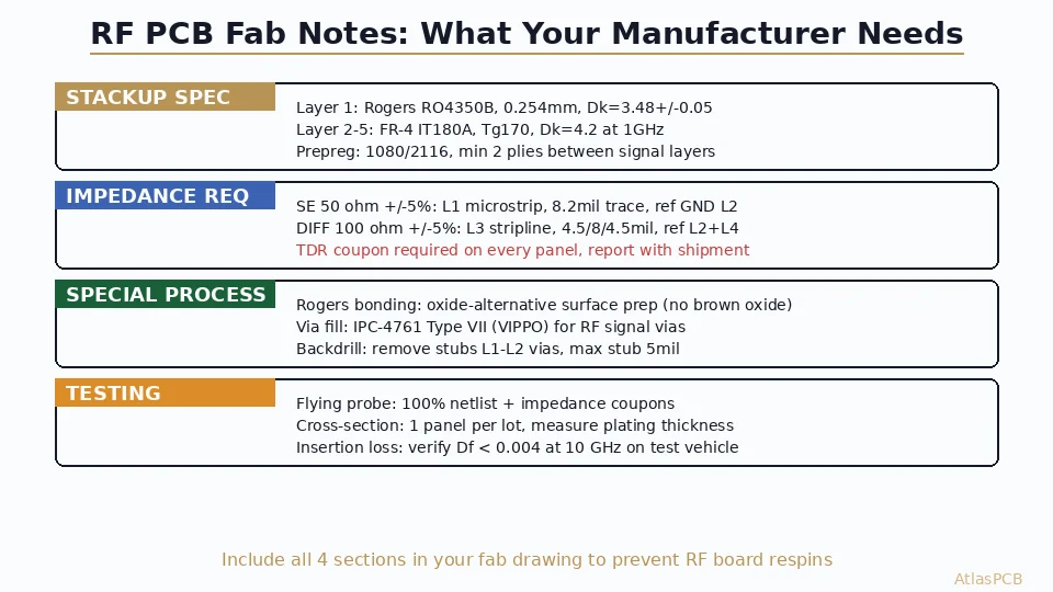
Class D: Single-ended 50 ohm +/-5% — RF signal path (2.4 GHz antenna feed). Microstrip on L1 referenced to L2 ground, Rogers RO4350B dielectric. Trace width: calculated by manufacturer based on actual material Dk characterization.
This classification approach tells your manufacturer exactly which traces need attention and what tolerance band applies to each group. It also allows them to prioritize coupon structures — they can build one coupon per impedance class rather than trying to test every unique trace width.
IMPEDANCE CONTROL EXPERTISE
Every Impedance Board Gets Engineering Review
Our process engineers verify your stackup calculations against our actual material properties before production. If adjustments are needed to hit your target impedance, we communicate changes with full simulation data — no surprises at incoming inspection.
Upload Gerber for DFM Review ›
Step 2: Stackup Table — The Critical Document
Your stackup table is the single most important document for impedance control. It communicates the physical structure that determines impedance, and it must be explicit enough that any competent manufacturer can build your board without guessing.
Here is what a proper impedance-controlled stackup table contains for a 6-layer design:
| Layer | Function | Cu Weight | Material | Thickness | Dk | Z0 Target |
|---|---|---|---|---|---|---|
| L1 | Signal (impedance) | 1 oz (finished) | — | 1.4 mil | — | 50 ohm SE |
| Prepreg | Dielectric | — | 2116 x1 | 4.5 mil | 4.2 | — |
| L2 | Ground (reference) | 0.5 oz | — | 0.7 mil | — | — |
| Core | Dielectric | — | FR-4 core | 20 mil | 4.5 | — |
| L3 | Signal (impedance) | 0.5 oz | — | 0.7 mil | — | 50 ohm diff |
| Prepreg | Dielectric | — | 2116 x2 | 9.0 mil | 4.2 | — |
| L4 | Power | 1 oz | — | 1.4 mil | — | — |
| Core | Dielectric | — | FR-4 core | 20 mil | 4.5 | — |
| L5 | Ground (reference) | 0.5 oz | — | 0.7 mil | — | — |
| Prepreg | Dielectric | — | 2116 x1 | 4.5 mil | 4.2 | — |
| L6 | Signal (impedance) | 1 oz (finished) | — | 1.4 mil | — | 50 ohm SE |
Critical notes to include below the table:
- “Manufacturer may adjust trace width by up to +/-0.5 mil to achieve target impedance with actual material Dk”
- “Prepreg thickness is post-lamination target — manufacturer to confirm with actual resin flow data”
- “Dk values from simulation are at 1 GHz. Manufacturer to use frequency-dependent Dk if available for their material”
- “Overall board thickness target: 62 mil +/-10%”
The reason for specifying Dk values explicitly is that different FR-4 suppliers have Dk ranging from 4.0 to 4.8 depending on glass style and resin content. If you designed your trace widths assuming Dk=4.2 and the manufacturer uses material with Dk=4.5, your 50-ohm trace becomes 53-54 ohms. By stating your assumption, you enable the manufacturer to compensate.
Step 3: Common Specification Mistakes That Cause Failures
Based on DFM reviews across thousands of impedance-controlled orders in our facility, these are the mistakes we catch most frequently:
Mistake 1: Specifying impedance without a reference layer. We see this on approximately 15% of new customer designs. The note says “50 ohm controlled impedance on L1” but does not state whether L2 is ground or power, or whether it is a continuous plane. If L2 has splits or cutouts under your impedance-controlled traces, the actual impedance will be significantly higher than target. Always state: “50 ohm microstrip on L1 referenced to L2 solid ground plane.”
Mistake 2: Using EDA default Dk values without verification. Altium’s built-in stackup manager defaults to Dk=4.5 for FR-4. If your manufacturer uses Isola 370HR (Dk=3.92 at 1 GHz) or Shengyi S1000-2M (Dk=4.25), the trace width calculated by Altium will produce incorrect impedance. Always ask your manufacturer: “What material will you use, and what is its Dk at my operating frequency?”
Mistake 3: Not specifying differential pair coupling geometry. Simply writing “100 ohm differential” is insufficient. The manufacturer needs to know: is it edge-coupled (traces side-by-side with controlled gap) or broadside-coupled (traces on adjacent layers)? What is the pair spacing? Is the coupling gap the same everywhere, or does it change at breakout regions? Document the coupling geometry explicitly.
Mistake 4: Ignoring copper roughness effects above 5 GHz. Standard oxide treatment adds 3-5 um of copper roughness. At 10+ GHz, this roughness increases conductor loss and shifts impedance by 2-5%. If you are designing above 5 GHz, specify: “Low-profile copper (Rz < 3 um) on impedance-controlled layers” or accept that you need to account for roughness in your margin.
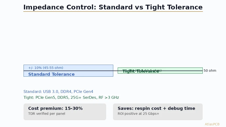
Mistake 5: Asking for +/-5% tolerance without understanding cost. Tighter tolerance requires tighter process controls: per-panel TDR verification, reduced etch variation windows, and sometimes rejection of panels that would pass +/-10%. Specify the tolerance that your design actually requires, not the tightest you can imagine. Most DDR4 designs work fine at +/-10%. PCIe Gen5 genuinely needs +/-7%.
DFM CHECK SERVICE
Catch Impedance Issues Before Production
We review every impedance-controlled design before it enters production. Common catches: missing reference plane designations, Dk mismatches, copper roughness omissions, and tolerance band optimization. Average review time: 4 hours from Gerber upload.
Submit Design for Review ›Step 4: Requesting TDR Verification and Test Reports
TDR (Time Domain Reflectometry) coupon measurement is the gold standard for impedance verification. A TDR sends a fast-rise pulse through a test trace and measures reflections caused by impedance discontinuities. The result is a measurement of characteristic impedance at every point along the trace.
When to request TDR verification:
- Any production run where impedance is functionally critical (not just “nice to have”)
- All boards destined for medical, aerospace, or automotive applications (IPC-6012 Class 3)
- When your impedance tolerance is +/-7% or tighter
- First article inspection on new designs
- Any time you are qualifying a new manufacturer
What to specify in your fab notes:
IMPEDANCE VERIFICATION REQUIREMENTS:
- TDR coupon measurement on every production panel
- Test coupons must replicate actual trace geometry (width, spacing, dielectric)
- Report format: TDR trace screenshot + numerical pass/fail table
- Acceptance criteria: within specified tolerance at all measured points
- Coupon location: panel margin, minimum 2 coupons per impedance class per panel
- Measurement equipment: TDR with <35 ps rise time
In our production, we build impedance coupons into the panel border automatically for every impedance-controlled order. We measure 100% of panels with a Polar CITS880s TDR system and include the report with shipment. Panels that fail coupon measurement are scrapped — we do not ship out-of-spec boards with a note saying “close enough.”
Step 5: Working with Your Manufacturer Collaboratively
The impedance specification process works best when it is collaborative rather than adversarial. The ideal workflow between designer and manufacturer looks like this:
Before PCB layout: Contact your target manufacturer and request their standard material offerings with characterized Dk values at your operating frequency. Design your stackup and trace widths using their actual material data, not generic textbook values. This eliminates the back-and-forth after Gerber submission.
During DFM review: Expect the manufacturer to propose adjustments. A 0.2 mil trace width change to compensate for actual vs. assumed Dk is normal and healthy. What matters is that they communicate the change, explain why, and get your approval before production. A manufacturer who never questions your stackup is either not checking or not experienced with impedance control.
After first article: Review the TDR report critically. Verify that measured impedance is centered within your tolerance band, not riding the edge. If your 50 ohm +/-10% board measures 54.5 ohm consistently, you should discuss trace width adjustment for subsequent lots even though it technically passes — you have no margin for material variation.
The manufacturers that excel at impedance control are the ones that invest in pre-production simulation. At AtlasPCB, we run every impedance stackup through our field solver before production, comparing our material’s measured Dk against your design assumptions. If there is a discrepancy, we contact you with simulation data showing the expected impedance with and without adjustment — giving you an informed choice rather than a surprise.
IMPEDANCE CONTROLLED PCB MANUFACTURER
Impedance Control Done Right, First Time
We process 200+ impedance-controlled designs per month across FR-4, Rogers, and hybrid stackups. Every order gets field-solver verification, per-panel TDR testing, and a detailed measurement report. Tolerance capability: +/-5% on Rogers, +/-7% on FR-4.
Summary: The Complete Impedance Specification
When you submit impedance-controlled Gerbers to a manufacturer, your documentation package should contain:
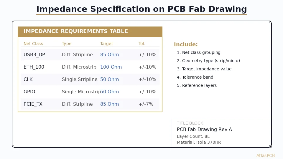
- Fab drawing with impedance requirements table (target Z, tolerance, reference layer, trace class)
- Stackup table with material type, Dk assumption, and dielectric thickness per layer
- Note authorizing manufacturer trace width adjustment within stated limits
- TDR verification requirement with acceptance criteria
- Test report delivery requirement
Getting this documentation right eliminates the primary source of impedance failures — communication gaps — and gives your manufacturer the information they need to build boards that meet spec on the first production run. The 30 minutes spent preparing a proper impedance specification saves weeks of respin time and thousands of dollars in failed prototypes.
ATLASPCB
Ready to Order Impedance-Controlled PCBs?
Upload your Gerbers and stackup. Our engineering team verifies impedance feasibility, proposes material-matched trace adjustments, and guarantees TDR-verified results on every production panel.
Get Instant Quote ›
Reviewed by AtlasPCB Engineering Team — 15+ years in advanced PCB fabrication for RF, HDI, and rigid-flex applications.
Related Reading:
About AtlasPCB — We specialize in complex PCB manufacturing for HDI, RF, and high-reliability applications. Explore our impedance-controlled PCB manufacturing, or get an free engineering DFM review . Every order includes free engineering review. Get your quote.
Reviewed by AtlasPCB Engineering Team — IPC-certified manufacturing specialists with 15+ years of production experience in HDI, RF, and high-reliability PCB fabrication. Content based on factory floor data and real customer design reviews.
Frequently Asked Questions
What tolerance should I specify for impedance-controlled PCBs?
Do I need to specify trace width, or will the manufacturer calculate it?
What is impedance coupon verification and when do I need it?
How do I specify differential impedance for USB or HDMI?
What information should I include in my fab drawing stackup table?
- impedance controlled PCB manufacturer
- PCB DFM check
- impedance specification
- controlled impedance design
- PCB stackup