· AtlasPCB Engineering · Engineering · 11 min read
JLCPCB vs Custom PCB Manufacturer for RF Boards: Why Budget Services Fail Above 5 GHz
Detailed comparison of JLCPCB and custom PCB manufacturers for RF circuit boards operating above 5 GHz. Covers material control, via transitions, insertion loss testing, and the hidden costs of RF board failures at mmWave frequencies.
Quick Answer
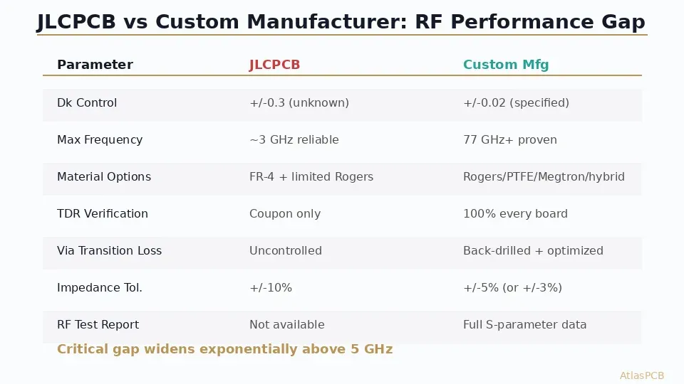
JLCPCB works for RF prototypes below 3 GHz, but above 5 GHz the uncontrolled dielectric properties, poor via transitions, and lack of RF verification make custom manufacturers essential — the performance gap grows exponentially with frequency, and a single failed RF board revision costs more than the entire production premium.
Quick Decision: JLCPCB or Custom Manufacturer for RF PCBs?
| Frequency Band | JLCPCB Viability | Custom Manufacturer Advantage |
|---|---|---|
| Below 2.4 GHz (BLE, Sub-GHz IoT) | Adequate for prototyping | Overkill unless production volume |
| 2.4-5 GHz (Wi-Fi 6, C-band) | Marginal — inconsistent results | Recommended for production |
| 5-10 GHz (Wi-Fi 7, X-band radar) | High failure risk | Essential — material control critical |
| 10-28 GHz (5G FR2, K-band) | Not viable | Required — hybrid stackup + backdrilling |
| 28-77 GHz (mmWave, automotive radar) | Impossible | Specialized process mandatory |
The short answer: if your RF traces carry signals above 5 GHz, JLCPCB is not a viable production path. The controlled variables that determine RF performance — dielectric constant stability, copper surface roughness, via stub resonance, and etch factor consistency — are simply not managed in a budget fabrication flow. The cost of discovering this through failed prototypes typically exceeds the lifetime premium of working with a dedicated RF PCB manufacturer from the start.
The Physics of Why Budget PCB Services Fail at RF Frequencies
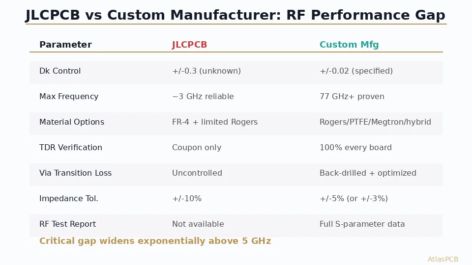
The fundamental challenge with RF PCB fabrication above 5 GHz is that every fabrication variable that a budget service leaves uncontrolled becomes a first-order contributor to signal degradation. At 1 GHz, a dielectric constant variation of +/-0.2 shifts your 50-ohm microstrip by about 2 ohms — annoying but manageable with matching networks. At 28 GHz, that same Dk variation creates impedance discontinuities that generate standing waves, increase insertion loss by 1-2 dB per inch, and destroy your noise figure budget.
In our facility, we track incoming laminate Dk at 10 GHz using a split-post dielectric resonator. We have measured lot-to-lot variation in standard FR-4 of 0.25 in Dk — which at 28 GHz corresponds to approximately 8% impedance shift on a microstrip line. Rogers 4350B, by contrast, arrives with certified Dk values at multiple frequencies, and our incoming QC confirms the laminate meets its +/-0.04 specification before any panel enters production. This single variable — knowing what your dielectric constant actually is — separates RF-capable fabrication from gambling.
The second critical factor is copper surface roughness. Standard FR-4 from budget fabricators uses electrodeposited copper with an Rz roughness of 5-8 um on the treated side. At 5 GHz, skin depth in copper drops to approximately 0.9 um — meaning the current flows almost entirely within the surface roughness peaks and valleys. The additional conductor loss from rough copper adds 0.3-0.5 dB/inch at 10 GHz compared to the rolled-annealed or HVLP (hyper-very-low-profile) copper that RF-focused manufacturers specify. By 28 GHz, this copper roughness penalty can account for 40% of total trace loss.
CHINA RF PCB MANUFACTURER
RF Boards from 2.4 GHz to 77 GHz
Rogers 4350B, PTFE, and hybrid stackups with 100% TDR and VNA verification on production panels.
Get RF PCB Quote ›
Via Transitions: The Silent RF Performance Killer
At frequencies below 3 GHz, a standard 0.3mm mechanical drill through a 1.6mm board creates a via with maybe 0.5 nH parasitic inductance and negligible stub resonance. Engineers can largely ignore via modeling and still get working hardware. This forgiving physics is why JLCPCB works perfectly fine for sub-GHz IoT modules and basic Wi-Fi designs.
Above 5 GHz, the via stub — the unused portion of a through-hole via extending beyond the signal layer — becomes a resonant antenna. A 1.0mm stub (typical for a signal transitioning on layer 2 of a 1.6mm board) resonates at approximately 37 GHz, with its first quarter-wave null creating a notch in the passband. Even at 10 GHz, this stub contributes 1-2 dB of insertion loss and creates an impedance discontinuity that reflects energy back toward the source.
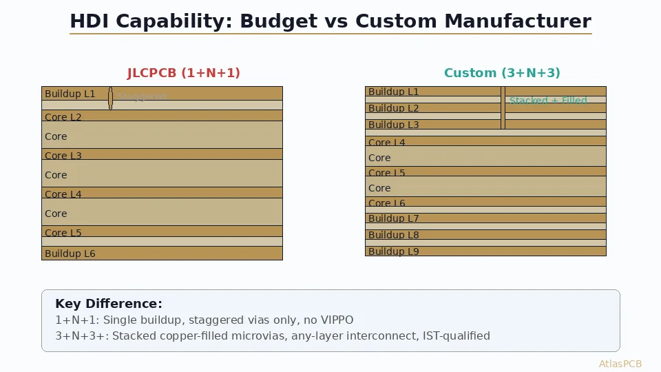
The solution is backdrilling — mechanically removing the via stub after plating. But backdrilling precision determines its effectiveness. JLCPCB does not offer backdrilling on standard orders. Even budget services that claim backdrilling capability typically achieve depth accuracy of +/-8 mil, which at 28 GHz leaves enough residual stub to create measurable return loss degradation.
Our process engineers control backdrill depth to +/-3 mil using laser depth measurement on each panel. For 77 GHz automotive radar boards, we routinely backdrill to within 4 mil of the target signal layer — leaving a 4-mil stub that only begins to resonate above 90 GHz. The difference between 4-mil and 12-mil residual stub at 77 GHz is approximately 4 dB of insertion loss improvement per via transition. On a typical radar front-end with 8-12 via transitions in the signal path, that is the difference between meeting and failing the system link budget.
Material System Control: What JLCPCB Cannot Guarantee
When you order a “Rogers 4350B” board from JLCPCB, you receive a board fabricated on Rogers 4350B laminate. What you do not receive is any guarantee about which lot that material came from, what the actual measured Dk of that specific sheet was, whether it was stored within humidity specifications before lamination, or how the hybrid bonding to FR-4 layers was characterized.
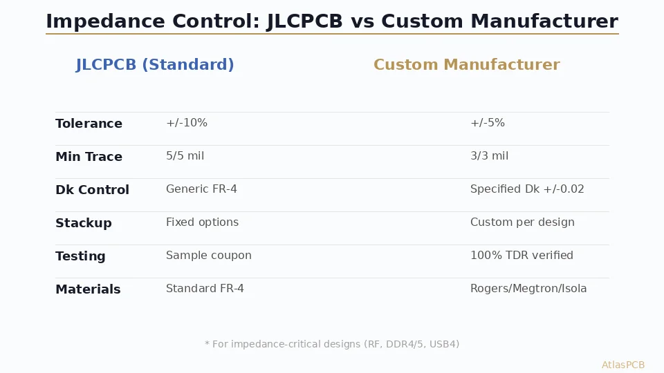
A custom RF PCB manufacturer manages the complete material chain. We maintain Rogers material inventory in humidity-controlled storage (below 50% RH, 23+/-2 C) and track each panel back to the specific laminate lot. When an engineer specifies Dk=3.48 at 10 GHz for their impedance calculation, we verify that the material in their panel measures within +/-0.04 of that value — because Rogers certifies it, and we confirm it.
The hybrid stackup is where budget services create the most unpredictable results. A Rogers/FR-4 hybrid board requires bonding dissimilar materials at specific temperatures and pressures. The prepreg between Rogers and FR-4 layers must be characterized for its contribution to the overall effective dielectric constant. In our process, we run test vehicles for each new hybrid stackup combination and document the effective Dk at 1, 5, 10, and 20 GHz — data that feeds directly into the customer’s impedance model.
JLCPCB processes hybrid boards using whatever bonding parameters their standard lamination profile allows. If the prepreg flow characteristics vary between lots (which they do — resin content typically varies 2-4% between batches), the as-fabricated dielectric properties shift. At 28 GHz, a 3% resin content change in the bonding prepreg can shift the effective Dk by 0.08 — enough to push a carefully designed 50-ohm GCPW line to 47 or 53 ohms.
ROGERS PCB MANUFACTURER
Certified Material Traceability for Every RF Panel
Rogers 4350B, 4003C, and PTFE with lot-level Dk certification and humidity-controlled storage.
Upload RF Stackup ›The True Cost of RF Board Failure
Engineers choosing JLCPCB for RF prototypes often frame the decision as “$50 vs $300 per board.” That arithmetic is correct for the unit cost. It completely ignores the cost of failure — which for RF boards above 5 GHz is not “the board doesn’t work” but rather “the board sort-of works, inconsistently, and you spend three weeks debugging phantom performance variations before discovering the root cause is fabrication variability.”
We have onboarded over 120 RF customers in the past two years who came to us after exactly this scenario. The typical story: engineer designs a 5.8 GHz front-end module, orders from JLCPCB, gets boards that measure -15 dB return loss on some channels and -8 dB on others. Assumes a layout issue, respins the board with adjusted trace widths. Second revision shows the same inconsistency. Third order from us with material control and TDR verification produces boards that consistently hit -20 dB return loss across all channels. The “savings” from two JLCPCB prototype runs cost the project 6-8 weeks of engineering time and a schedule slip that delayed market entry.
For production volume, the math becomes even clearer. A 1000-unit production run of a 5G small cell front-end on Rogers 4350B costs approximately $45/board from a custom manufacturer vs $15/board from a budget service — a $30,000 premium for the run. One field failure requiring a recall, root-cause investigation, redesign, and re-qualification costs $150,000-500,000 depending on the application. The insurance value of proper RF fabrication is not a luxury; it is basic risk management.
When JLCPCB Actually Makes Sense for RF Projects
Not every RF project needs a custom manufacturer. JLCPCB serves a legitimate role in the RF development workflow for specific use cases:
Early-stage concept validation below 3 GHz works well on JLCPCB’s standard FR-4 service. If you are designing a LoRa module at 915 MHz or a Bluetooth Low Energy beacon, the wavelengths are long enough that fabrication variations barely affect performance. Get your layout verified, confirm basic functionality, and move on.
Antenna prototype iteration is another valid use case. If you are optimizing a patch antenna geometry through multiple design iterations, the absolute gain matters less than the relative improvement between revisions. JLCPCB’s consistency within a single order batch is reasonable — the problem is batch-to-batch variation and the absence of absolute calibration.
Test fixtures and evaluation boards that interface to RF components but do not carry the primary RF signal path can safely use budget fabrication. Your LNA evaluation board that breaks out SMA connectors to a 2-inch microstrip does not need +/-3 mil backdrill control.
The decision framework is straightforward: if the RF performance of the PCB directly determines whether your product passes its system-level specifications, use a custom manufacturer. If the PCB is a tool for evaluating something else, JLCPCB is fine.
IMPEDANCE CONTROLLED PCB MANUFACTURER
From Prototype to Production — Same RF Quality
Consistent performance from first prototype through 10,000-unit production. No surprises at volume.
RF Verification: What Your Test Report Should Include
A custom RF PCB manufacturer provides verification data that budget services simply do not generate. For any board operating above 5 GHz, you should expect:
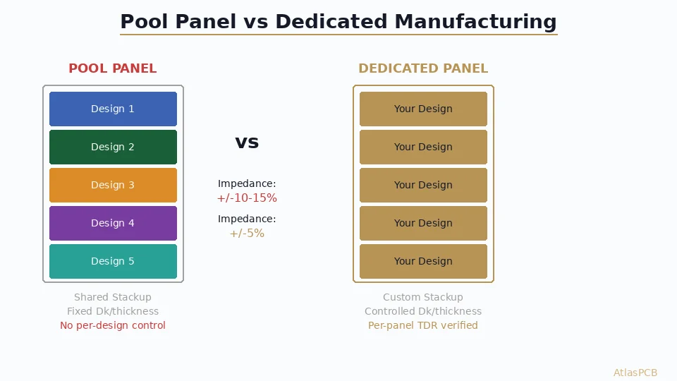
TDR (Time Domain Reflectometry) impedance data on every production panel, not just a test coupon at the panel edge. The coupon might measure 50.2 ohms while the actual board trace — with its unique etch factor, proximity to ground voids, and thermal relief influence — measures 47.8 ohms. Panel-level TDR catches this.
Insertion loss measurement on a dedicated test coupon with known length, allowing extraction of the per-inch loss at your operating frequency. We run stripline and microstrip test traces at 5, 10, 20, and 40 GHz on every Rogers or PTFE panel, providing the customer with measured loss data they can compare against their simulation.
Cross-section analysis documenting actual trace width (top and bottom), etch factor, copper thickness, and dielectric height. These physical measurements feed back into the impedance model to confirm that the as-fabricated geometry matches the design intent.
Backdrill depth verification through X-ray or destructive cross-section, confirming that via stubs are within specification. For automotive radar boards, we measure every backdrill on a statistical sample using automated X-ray inspection and report Cpk data.
None of this data exists in a JLCPCB order. You receive boards — and the implicit assumption that they meet your specifications, with no evidence either way.
ATLASPCB
Ready to Build RF Boards That Work the First Time?
Upload your Gerber files and stackup. Our RF process engineers review every design for manufacturability before quoting.
Upload Gerber Files ›
Reviewed by AtlasPCB Engineering Team — 15+ years in advanced PCB fabrication for RF, HDI, and rigid-flex applications.
Related Reading:
About AtlasPCB — We specialize in complex PCB manufacturing for HDI, RF, and high-reliability applications. Explore our RF and high-frequency PCB services . Every order includes free engineering review. Get your quote.
Reviewed by AtlasPCB Engineering Team — IPC-certified manufacturing specialists with 15+ years of production experience in HDI, RF, and high-reliability PCB fabrication. Content based on factory floor data and real customer design reviews.
Frequently Asked Questions
Can JLCPCB make RF PCBs for 5G applications?
What makes a custom PCB manufacturer better for RF boards?
How much more does a custom RF PCB cost compared to JLCPCB?
At what frequency does JLCPCB stop being viable for RF boards?
- rf-pcb
- jlcpcb-comparison
- pcb-manufacturing
- high-frequency