· Sophia Reyes · Engineering · 8 min read
PCB Impedance Coupon Design and TDR Testing
Learn how to design impedance test coupons, interpret TDR results, and specify controlled impedance PCBs. Covers IPC-2141A coupon types, stripline vs microstrip validation, and common impedance failure root causes.
Quick Answer
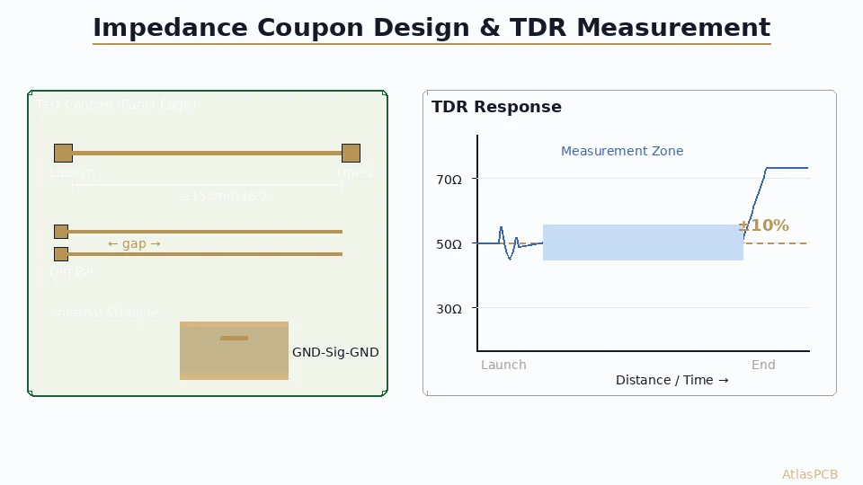
PCB impedance coupons are dedicated test structures fabricated on the same panel as production boards, measured with Time-Domain Reflectometry (TDR) to verify controlled impedance traces meet their ±10% target. Proper coupon design requires matching the production stackup layer-by-layer, using IPC-2141A-compliant structures with sufficient trace length (≥150mm for TDR), and positioning coupons at multiple panel locations to capture dielectric thickness variation across the panel.
Why Impedance Coupons Matter
Every controlled-impedance PCB leaves the factory with a test report. But what exactly is being measured, and how do you know the coupon actually represents your production traces?
The impedance coupon is the only manufacturing verification that confirms your stackup delivers the target impedance. Unlike electrical testing (which checks continuity) or cross-sectioning (which verifies geometry at one point), TDR coupon testing validates the electromagnetic behavior of the transmission line over its full length.
For designs running at USB 3.2 (10 Gbps), PCIe Gen 5 (32 GT/s), or DDR5 (6400 MT/s), a 5Ω impedance deviation can push insertion loss above budget and create compliance failures. Understanding coupon design and TDR interpretation lets you catch problems at bare-board stage rather than during system-level validation.
TDR Fundamentals for PCB Engineers
How TDR Works
Time-Domain Reflectometry sends a fast-rising voltage step into a transmission line and measures the reflected signal:
- Step generator produces a pulse with 20-35ps rise time
- Sampling head captures the incident + reflected waveform
- Impedance calculation: Z = Z₀ × (1 + ρ) / (1 - ρ), where ρ is the reflection coefficient
- Display shows impedance versus distance (propagation time)
The spatial resolution of a TDR measurement is approximately:
- Resolution = (rise time × propagation velocity) / 2
- For 35ps TDR and FR-4 (v ≈ 0.55c): Resolution ≈ 2.9mm
This means impedance features smaller than ~3mm appear as averaged in the TDR trace. Coupon design must account for this resolution limit.
TDR vs. VNA for Impedance Verification
| Parameter | TDR | VNA |
|---|---|---|
| Measures | Impedance vs. distance | S-parameters vs. frequency |
| Spatial resolution | ~3mm (35ps system) | Full line average |
| Setup time | Minutes | 15-30 min (calibration) |
| Coupon requirement | Single-ended access | Two-port calibration structures |
| Industry standard | IPC-TM-650 2.5.5.7 | IPC-TM-650 2.5.5.12 |
| Cost per test | $5-15 | $50-200 |
For production screening, TDR is the universal standard. VNA is used for characterization and correlation studies.
IPC-2141A Coupon Types
IPC-2141A (Design Guide for High-Speed Controlled Impedance Circuit Boards) defines standard coupon architectures:
Type A — Single-Ended External (Microstrip)
Signal trace on outer layer, reference plane below
┌─────────────────────────────────┐
│  ═══════════════════════════════ │ ← Signal (Layer 1)
│  ─────────────────────────────── │ ← Reference GND (Layer 2)
│  Dielectric: h = 3.5-5.0 mil   │
└─────────────────────────────────┘
Design requirements:
- Trace width: per stackup calculation (typically 4-6 mil for 50Ω)
- Trace length: ≥150mm
- Distance from reference plane edge: ≥5× dielectric thickness
- Distance from other signals: ≥3× trace width
Type B — Single-Ended Internal (Stripline)
Signal trace embedded between two reference planes
┌─────────────────────────────────┐
│  ─────────────────────────────── │ ← Reference GND (Layer N-1)
│  ═══════════════════════════════ │ ← Signal (Layer N)
│  ─────────────────────────────── │ ← Reference GND (Layer N+1)
└─────────────────────────────────┘
Design requirements:
- Trace width: per stackup calculation (typically 3.5-5 mil for 50Ω)
- Balanced dielectric: equal thickness above and below for symmetric stripline
- Note: asymmetric (offset) stripline requires adjusted trace width
Type C — Differential External (Edge-Coupled Microstrip)
Two coupled traces on outer layer
┌─────────────────────────────────┐
│  ═══  gap  ═══════════════════  │ ← P/N pair (Layer 1)
│  ─────────────────────────────── │ ← Reference GND (Layer 2)
└─────────────────────────────────┘
Design requirements:
- Differential impedance: typically 85Ω (USB), 85-100Ω (PCIe, DDR)
- Gap (space): critical parameter — measure both trace width AND gap
- Coupon must use same space as production routing
- Length matching: P and N traces within 2 mil of each other
Type D — Differential Internal (Broadside or Edge-Coupled Stripline)
Edge-coupled differential stripline
┌─────────────────────────────────┐
│  ─────────────────────────────── │ ← Reference GND
│  ═══  gap  ═══════════════════  │ ← P/N pair
│  ─────────────────────────────── │ ← Reference GND
└─────────────────────────────────┘
Designing Effective Impedance Coupons
Coupon Placement on Panel
Coupon position matters because PCB manufacturing introduces systematic variation:
- Dielectric thickness: Prepreg flow is thinner at panel center (higher pressure), thicker at edges
- Etch uniformity: Chemical etch rates vary across panel — center vs. edge can differ 5-15%
- Plating distribution: Electroplated copper thickness varies with current density distribution
Best practice: Place coupons at 2-4 locations to bracket the production board locations. Always include one coupon at the panel position closest to your most critical impedance traces.
Launch Design (Critical!)
The launch is the transition from the TDR probe contact point to the coupon trace. Poor launches mask the true line impedance:
SMA Launch (Coaxial):
- Best accuracy (<1Ω error)
- Requires drilled via + ground ring
- Expensive — typically used for characterization only
Pad Launch (Standard Production):
- Probe lands on a rectangular pad connected to the trace
- Pad creates a capacitive discontinuity (lowered impedance bump in TDR)
- Design pad as small as possible: 0.8mm × 1.2mm maximum
- Add anti-pad relief in adjacent ground planes to compensate
GSG (Ground-Signal-Ground) Probe Launch:
- Used with microwave probes for frequencies >10 GHz
- Requires coplanar ground pads adjacent to signal pad
- Pitch must match available probe (150µm, 200µm, or 250µm standard)
Trace Length Considerations
The coupon trace must be long enough for the TDR to resolve:
- Minimum length: 150mm (6”) for 35ps TDR — provides ~1ns of readable data
- Recommended length: 200-250mm — allows averaging over measurement window
- Maximum practical: 300mm — beyond this, conductor loss attenuates the TDR step
For differential pairs, maintain the exact same length for P and N traces throughout the coupon.
Precision Impedance Control
±5% Impedance Tolerance Available
AtlasPCB offers standard ±10% and high-precision ±5% controlled impedance with full TDR reports. We design and verify coupons to match your exact stackup.
Request Impedance Stackup Review →Interpreting TDR Results
Reading the TDR Waveform
A typical TDR trace shows:
- System impedance (first segment): 50Ω from the instrument cable
- Connector/probe transition: Capacitive dip or inductive spike
- Launch region: 2-5mm of transitional impedance (ignore for specification compliance)
- Trace region: The measurement zone — should be flat at target impedance
- Open-circuit reflection: Rising to 2× impedance at unterminated end
Where to read the impedance: The IPC-TM-650 method specifies reading the impedance in the “flat zone” between the launch transition and the end reflection. Typically 20-80% of the trace length.
Common TDR Patterns and Root Causes
Impedance trending upward along trace: Trace width narrowing (etch taper from chemical etch directionality)
Impedance trending downward: Dielectric thinning along trace direction, or progressive copper thickness increase from plating
Periodic ripples: Glass weave effect — trace crosses glass bundles and resin-rich gaps creating local Er variation. Period matches weave pitch (~1.2mm for 1080, ~2.1mm for 2116)
Sharp dips at regular intervals: Return path discontinuities — antipad clearances or splits in reference plane
Offset between P and N traces (differential): Asymmetric etch, one trace consistently wider than the other
Process Variables That Affect Impedance
Etch Factor
Chemical etching removes copper isotropically — undercutting the resist creates trapezoidal trace cross-sections:
- 1 oz copper base: Etch back ≈ 0.5-0.8 mil per side
- 2 oz copper: Etch back ≈ 1.0-1.5 mil per side
- Final trace width = artwork width - (2 × etch back)
Impact: A 4.0 mil artwork line might etch to 3.0 mil actual width, increasing impedance by 8-12Ω.
Mitigation: Fabricator adds etch compensation to artwork. Coupon validates that compensation is correct.
Dielectric Constant Variation
FR-4 is not homogeneous — it’s woven glass in resin matrix:
- Glass bundles: Er ≈ 6.2 (high permittivity)
- Resin pockets: Er ≈ 3.2 (low permittivity)
- Composite Er: 3.8-4.5 depending on glass content and resin fill
Glass weave effect: Traces aligned along glass bundles see higher effective Er (lower impedance) than traces over resin-rich gaps. This creates ±3-5% impedance variation within a single board.
Mitigation: Use spread-glass prepreg (e.g., 1078 or NE glass) for critical impedance layers. Rotate trace direction relative to weave.
Soldermask Loading
Outer-layer microstrip coupons should be tested with soldermask applied, because production boards will have mask:
- Soldermask adds 2-5Ω capacitive loading to microstrip
- If coupon is tested before mask, impedance reads 2-5Ω too high
- Specify “test after soldermask” for outer layers in fabrication notes
Copper Roughness
Copper foil surface roughness increases effective conductor length:
- Standard electrodeposited (ED): Rz = 5-8 µm
- Low-profile (LP): Rz = 3-5 µm
- Very-low-profile (VLP/HVLP): Rz = 1.5-3 µm
Roughness effects become significant above 5 GHz. For GHz-range impedance-controlled traces, specify VLP copper and adjust field solver roughness parameters.
Specifying Impedance in Fabrication Notes
Minimum Specification Information
Your fab notes should include:
CONTROLLED IMPEDANCE REQUIREMENTS:
Layer 1 (Microstrip): 50Ω ±10%, single-ended
Layer 3 (Stripline):  50Ω ±10%, single-ended
Layer 1 (Microstrip): 90Ω ±10%, differential, 5mil gap
Layer 3 (Stripline):  100Ω ±10%, differential, 5mil gap

Reference: IPC-2141A coupon per IPC-TM-650 2.5.5.7
Report: TDR report required with each lot delivery
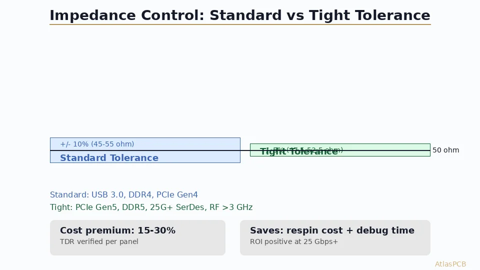
Tolerance: ±10% of nominal (±5% available on request)

Notes:
- Coupon must match production stackup exactly
- Test outer layers after soldermask application
- Provide etch cross-section with first article
Tolerance Considerations
Standard ±10% is achievable by most fabricators. ±7% requires:
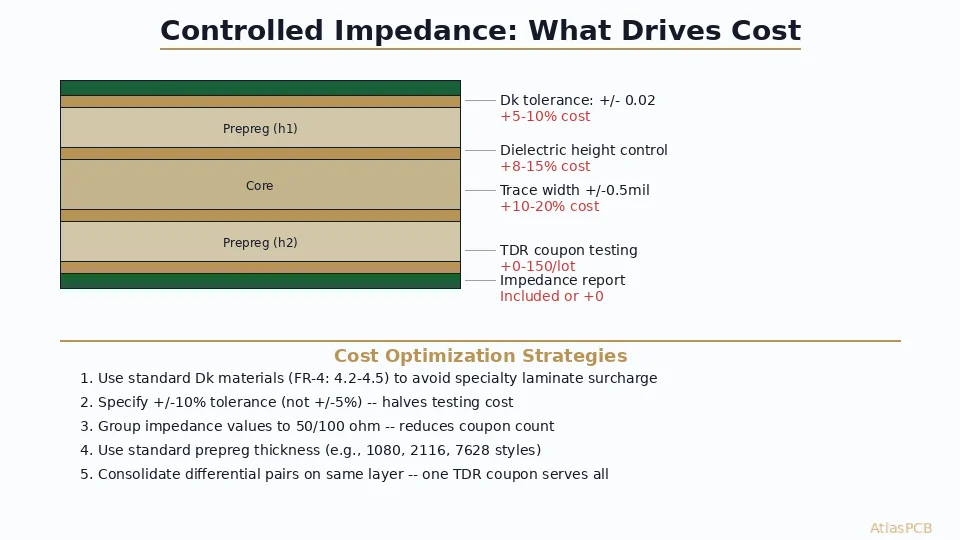
- Tighter prepreg thickness control (±0.5 mil vs. ±1.0 mil)
- Etch compensation feedback loop
- Panel-level impedance mapping
±5% requires:
- Laser direct imaging (LDI) for trace definition
- Spread-glass or low-Dk prepreg
- Statistical process control with Cpk >1.33
Cross-Sectioning: The Complementary Validation
While TDR measures electromagnetic behavior, cross-sectioning reveals physical geometry:
What to measure:
- Trace width (top and bottom of trapezoid)
- Trace thickness
- Dielectric height to reference plane
- Copper roughness profile
Correlation: Field solver prediction → Cross-section geometry → TDR measurement should all agree within 3-5Ω. Systematic disagreement indicates a modeling error (wrong Er, unaccounted roughness, or missing soldermask in model).
Advanced Topics
De-embedding Launch Parasitics
For precision measurements (<±2Ω accuracy), the launch discontinuity must be mathematically removed:
- Measure a “short” reference coupon (pad + 5mm trace + short)
- Use TDR software to de-embed the launch reflection
- Report only the de-embedded trace impedance
Most production testing does NOT de-embed — the launch is included in the ±10% budget. Specify de-embedded measurement only for Class 3+ applications.
Temperature Effects
Impedance shifts with temperature due to Er changes:
- FR-4 Er increases ~0.01 per 10°C increase
- Net effect: impedance decreases ~0.5-1Ω per 50°C rise
Production TDR is performed at room temperature (23±5°C). Operating temperature impedance can be calculated from the coupon data using the Er temperature coefficient.
Further Reading
- Controlled Impedance PCB Stackup Design Rules
- Differential Pair Routing: Tight vs Loose Coupling
- PCB Impedance Matching for Differential Pairs
- RF Transmission Line Loss Budgeting for 5G/mmWave
Need controlled impedance manufacturing? Get a quote with your stackup requirements. AtlasPCB provides full TDR reports with every controlled-impedance delivery and supports impedance tolerances from ±10% down to ±5%.
About AtlasPCB — We specialize in complex PCB manufacturing for HDI, RF, and high-reliability applications. Explore our impedance-controlled PCB manufacturing, or get an full PCB manufacturing capabilities . Every order includes free engineering review. Get your quote.
Reviewed by AtlasPCB Engineering Team — IPC-certified manufacturing specialists with 15+ years of production experience in HDI, RF, and high-reliability PCB fabrication. Content based on factory floor data and real customer design reviews.
Frequently Asked Questions
What is the minimum trace length for a TDR impedance coupon?
How many impedance coupons should I specify per panel?
Why does my measured impedance not match the field solver prediction?
- impedance-control
- tdr-testing
- pcb-testing
- signal-integrity
- ipc-2141
- coupon-design