· AtlasPCB Engineering · Engineering · 10 min read
JLCPCB vs Custom PCB Manufacturer for HDI and Rigid-Flex: Where Budget Fabs Hit Their Ceiling
A detailed technical comparison of JLCPCB's HDI and rigid-flex capabilities versus what a dedicated custom PCB manufacturer delivers — covering microvia reliability, sequential lamination limits, polyimide flex construction, and engineering oversight.
Quick Answer
JLCPCB handles basic 1+N+1 HDI with single-stage laser drilling and does not offer rigid-flex construction. For designs requiring 2+N+2 or higher HDI buildups with stacked microvias, via-in-pad, or any rigid-flex PCB with controlled impedance on flex layers, a custom manufacturer with sequential lamination expertise and polyimide process control is required.
Quick Answer: Where JLCPCB’s HDI and Flex Capabilities End
| Capability | JLCPCB | Custom HDI/Flex Manufacturer |
|---|---|---|
| HDI Buildup | 1+N+1 only | Up to 5+N+5 (any-layer) |
| Microvia Type | Staggered, unfilled | Stacked, copper-filled, capped |
| Min Laser Drill | 0.1mm | 0.075mm |
| Via-in-Pad | Limited (no planarization) | Full VIPPO (plated, filled, planarized) |
| Rigid-Flex | Not available | Up to 22 layers, 1-6 flex sections |
| Impedance on Flex | N/A | Controlled to +/-7% on polyimide cores |
| Sequential Lamination Stages | 1 | Up to 5 |
| Microvia Reliability Testing | None reported | IST + microsection per panel |
If your design requires anything in the right column, JLCPCB cannot be your manufacturer. The gap is not about price — these processes require fundamentally different production equipment and engineering workflows.
The HDI Divide: Why 1+N+1 Is Not Really “HDI Manufacturing”
The term HDI gets applied broadly in the budget fab market, but there is a meaningful technical boundary between single-stage laser drilling and true sequential lamination HDI. Understanding this boundary saves engineers from committing to a manufacturer that cannot fabricate their design.
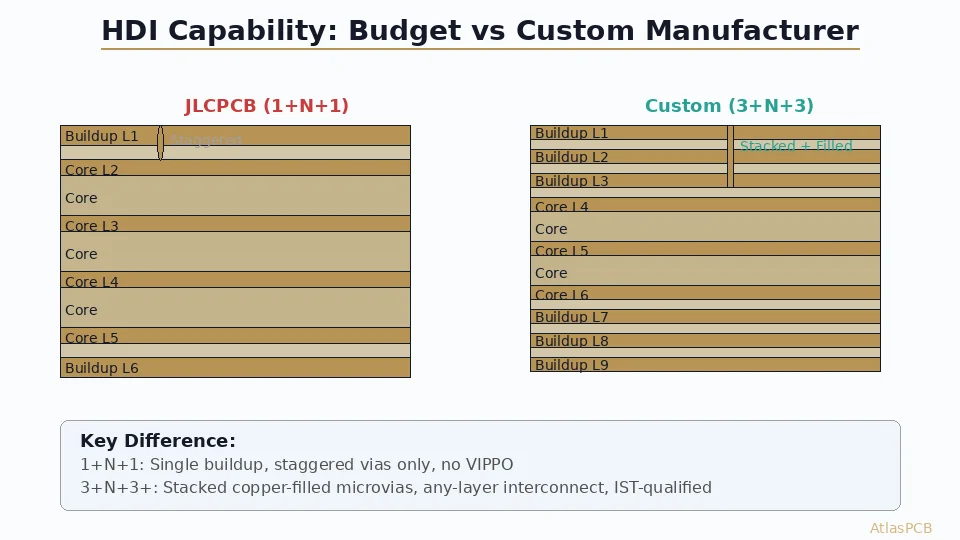
JLCPCB’s 1+N+1 offering adds one buildup layer per side to a conventional core. The laser drills microvias from layer 1 to layer 2 and from the last layer to the second-to-last layer. These microvias are staggered — meaning a via on the top buildup layer cannot land directly on a via in the core. This constraint limits routing escape options for fine-pitch BGAs and prevents true vertical interconnect stacking.
In our production facility, approximately 40% of HDI orders require 2+N+2 or higher builds. The reason is straightforward: modern SoC and FPGA packages at 0.5mm pitch with 400+ balls simply cannot break out through a single microvia layer. You need at least two sequential buildup stages to provide enough routing channels between ball pads. Once you reach 0.4mm pitch or multi-die modules, 3+N+3 becomes the minimum practical configuration.
The manufacturing difference is substantial. Each sequential lamination stage requires a complete press cycle — layup, lamination at controlled temperature/pressure profiles, laser drilling, desmear, copper plating, and pattern imaging. A 3+N+3 board goes through the press three additional times compared to a conventional multilayer. This demands precise registration between stages (typically 25-37 microns), z-axis depth control during laser ablation, and process engineering to manage cumulative thermal stress.
HDI MANUFACTURING EXPERTISE
Up to 5+N+5 HDI with Stacked Microvias
Sequential lamination, copper-filled vias, IST-verified reliability. Process engineering review included with every HDI order.
Upload Your HDI Design ›
Stacked Microvias vs Staggered: The Reliability Gap
The distinction between stacked and staggered microvias is not merely an aesthetic routing preference — it directly impacts electrical performance and long-term reliability.
Staggered microvias offset each layer’s via by 150-200 microns from the one below it. This works adequately for simple signal routing but consumes lateral real estate and creates longer current paths for power delivery. More critically, staggered configurations cannot support the via-in-pad requirement that virtually all fine-pitch BGA packages demand for proper solder joint formation.
Stacked microvias place each subsequent layer’s via directly on top of the previous one, creating a vertical column through multiple buildup layers. This requires the lower microvia to be copper-filled and planarized before the next buildup layer is laminated on top. The copper fill process — electroplating the laser-drilled hole to full copper density, then surface-planing to flatness within 10 microns — is the critical step that budget manufacturers skip.
From a reliability standpoint, we routinely test stacked microvia structures through 6x reflow simulation (peak 260C for lead-free processes) followed by 500-cycle thermal shock between -55C and +125C. The failure mode for improperly filled microvias is barrel cracking at the interface between the copper fill and the capture pad, which manifests as intermittent open circuits that worsen with thermal cycling. In our experience reviewing competitor panels, roughly 15-20% of stacked microvia structures from manufacturers without proper fill process control show some degree of voiding visible in microsection analysis.
Rigid-Flex: A Capability JLCPCB Simply Does Not Offer
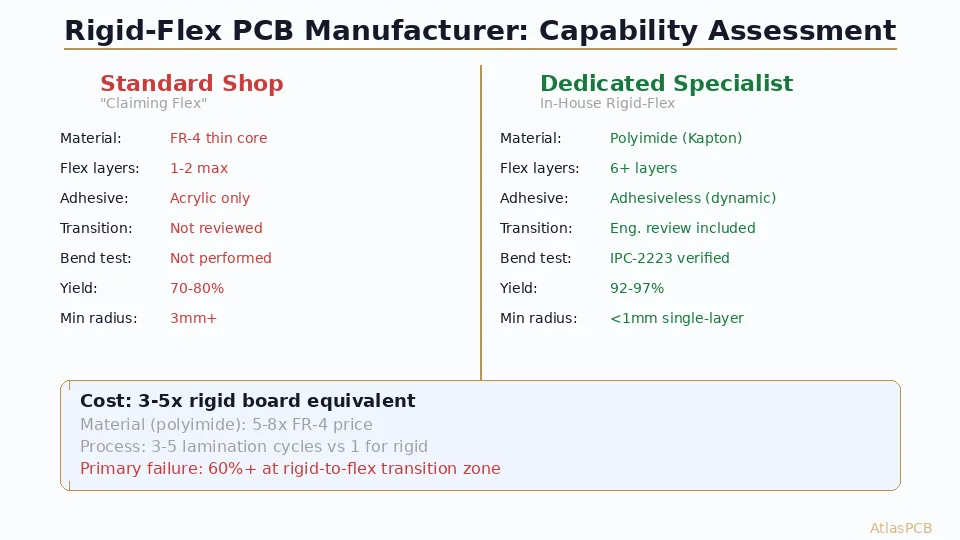
Rigid-flex PCB manufacturing is not an incremental upgrade from rigid board production — it requires entirely separate production equipment, materials handling procedures, and process engineering expertise. This is why JLCPCB, despite their scale, has not added it to their capability list.
The fundamental challenge is integrating polyimide flex cores (typically Dupont AP or Panasonic FELIOS) with rigid FR-4 or high-Tg sections while maintaining controlled peel strength at the flex-to-rigid transition zone. The lamination cycle for a rigid-flex is significantly more complex than a standard multilayer: temperature ramp rates must be carefully controlled to prevent polyimide delamination, pressure must be uniform across the panel despite varying layer counts between rigid and flex zones, and adhesive systems (either acrylic or epoxy-based bondply) must be selected for the target flexibility cycle life.
In our rigid-flex production, the most common design we fabricate is a 6-8 layer board with 2 flex layers, typically for medical wearables, aerospace avionics, or defense electronics where connector elimination improves reliability. The flex zones typically require 0.1mm polyimide cores with rolled annealed copper at 12-18 micron thickness — not the standard electrodeposited copper used in rigid sections. This dual-copper specification alone means the manufacturer needs separate material inventory and press programs.
The engineering review for rigid-flex is substantially more involved than rigid boards. We check bend radius adequacy (minimum 6x the flex section thickness for dynamic applications), verify that traces route perpendicular to the bend axis, confirm stiffener placement doesn’t create stress concentration points, and validate that the coverlay opening geometry allows proper component mounting in transition zones.
RIGID-FLEX SPECIALISTS
From Concept to Qualified Rigid-Flex in 18 Days
Polyimide flex cores, controlled impedance on flex layers, dynamic bend qualification. We review your flex-zone design before production.
Real-World Decision Scenarios
Scenario 1: 0.5mm BGA Breakout for an FPGA Module
Your design uses a Xilinx Kintex UltraScale FPGA with a 676-ball BGA at 0.5mm pitch. The breakout requires two microvia layers on top and bottom to escape all signal pins to inner routing layers. The BGA pad design requires via-in-pad with copper fill and planarization.
JLCPCB result: Cannot fabricate. Their 1+N+1 HDI cannot provide 2-stage breakout, and their via-in-pad process does not include proper planarization for 0.5mm pitch reflow reliability.
Custom manufacturer result: Standard 2+N+2 HDI build with VIPPO (Via-In-Pad Plated Over). 10-layer stackup with 0.075mm laser vias, copper-filled and planarized to less than 10 microns surface variation. Panel includes IST coupons for reliability qualification.
Scenario 2: Medical Device with Flex Interconnect
A patient monitoring device requires a 4-rigid-section board connected by 3 flex zones, folding into a compact enclosure. Two flex zones are dynamic (continuous bending during use), one is static (bent once during assembly). Total layer count: 8 rigid layers, 2 flex layers carrying differential impedance-controlled USB 2.0 signals.
JLCPCB result: Not possible. Rigid-flex is not offered.
Custom manufacturer result: 8+2 rigid-flex with polyimide flex cores, controlled impedance to +/-7% on flex layers using coverlay-compensated stackup simulation, dynamic bend-rated materials (rolled annealed copper, acrylic adhesive bondply for >100,000 cycle life).
Scenario 3: Dense IoT Module with 0.4mm Pitch CSP
A compact BLE module uses a WLCSP package at 0.4mm pitch with 80 balls. Board size is 12x12mm. The routing density requires 3+N+3 HDI to break out all signals in a 6-layer stackup.
JLCPCB result: Cannot fabricate. 0.4mm pitch breakout requires stacked vias through 3 buildup layers — far beyond 1+N+1 capability.
Custom manufacturer result: 3+N+3 HDI, 6-layer stackup, 0.075mm laser vias stacked three deep, total board thickness 0.8mm. Any-layer HDI interconnect allows maximum routing flexibility in the ultra-compact form factor.
ENGINEERING REVIEW
Not Sure If Your Design Needs Custom HDI?
Upload your Gerber files — our process engineers assess manufacturability and recommend the optimal HDI configuration within 24 hours.
Submit for Review ›The Cost Question: Is Custom Always More Expensive?
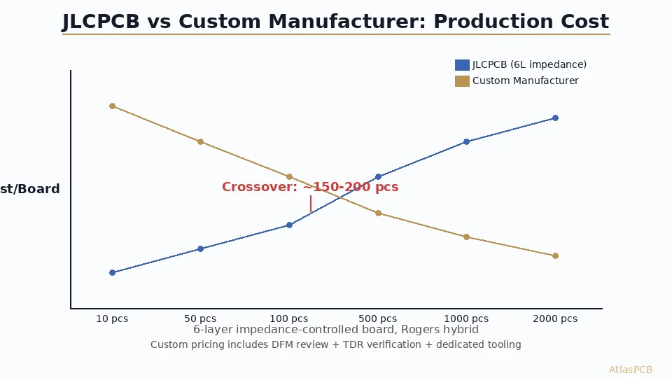
The assumption that JLCPCB is always cheaper deserves examination. For standard 2-4 layer FR-4 prototypes with relaxed specs, JLCPCB’s pricing is genuinely difficult to beat — $2-5 for 5 boards. But the pricing landscape shifts dramatically once advanced features enter the picture.
JLCPCB’s 1+N+1 HDI carries a significant surcharge over their standard multilayer pricing. A 6-layer HDI board costs $35-80 per panel in prototype quantities. At that price point, custom manufacturers offering 2+N+2 HDI with proper stacked microvias, copper fill, and engineering review are competitive at $80-150 per panel. The custom manufacturer delivers substantially more capability for only 2-3x the cost, and that cost delta drops rapidly at production volumes (100+ panels).
For rigid-flex, since JLCPCB doesn’t offer it, the real comparison is against the alternative approach: rigid PCB plus FPC connector. A rigid-flex prototype (5 pcs) at 8-layer with 2 flex zones typically costs $1,200-2,000 from a qualified manufacturer. The alternative — separate rigid board ($50) plus FPC ($30) plus connector ($5-15 each, both sides) — costs less in BOM but adds assembly labor, connector failure risk, and system thickness. For medical and aerospace applications where connector failure is unacceptable, rigid-flex eliminates a reliability risk that justifies the fabrication premium.
Making the Decision: A Framework
The decision is not really “JLCPCB vs custom” — it’s about matching your design requirements to the right tier of manufacturer capability.
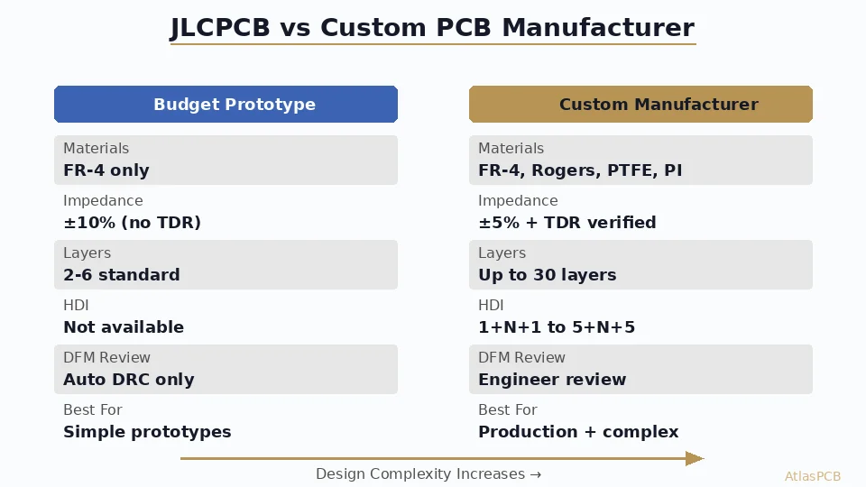
Use JLCPCB when all of these are true: standard FR-4 material, no more than 1+N+1 HDI (or conventional through-hole only), impedance tolerance of +/-10% is acceptable, no rigid-flex sections, no specialty surface finishes beyond ENIG, prototype quantities under 50 pieces, and the design has no reliability qualification requirements.
Switch to a custom manufacturer when any one of these applies: HDI buildup exceeds 1+N+1, the design includes any rigid-flex sections, impedance control tighter than +/-7% is required, Rogers or PTFE materials are needed for RF sections, the application requires IPC Class 3 or aerospace qualification, production volumes where per-unit engineering support amortizes across quantity, or your design pushes any single specification beyond standard capability.
The gap between budget and custom PCB manufacturing is not about quality of execution at similar specs — JLCPCB produces good boards within their capability window. The gap is about the ceiling of that capability window and the engineering support that prevents costly design respins.
ATLASPCB
Ready for HDI or Rigid-Flex That Works First Time?
Upload your design. Our engineers confirm manufacturability, optimize your stackup, and deliver boards with IST-verified reliability documentation.
Get Your Quote ›
Reviewed by AtlasPCB Engineering Team — 15+ years in advanced PCB fabrication for RF, HDI, and rigid-flex applications.
Related Reading:
About AtlasPCB — We specialize in complex PCB manufacturing for HDI, RF, and high-reliability applications. Explore our HDI PCB manufacturing capabilities, or get an rigid-flex PCB manufacturing . Every order includes free engineering review. Get your quote.
Reviewed by AtlasPCB Engineering Team — IPC-certified manufacturing specialists with 15+ years of production experience in HDI, RF, and high-reliability PCB fabrication. Content based on factory floor data and real customer design reviews.
Frequently Asked Questions
Can JLCPCB make HDI PCBs with stacked microvias?
Does JLCPCB offer rigid-flex PCB manufacturing?
What HDI microvia reliability testing does a custom manufacturer provide?
When is 1+N+1 HDI sufficient versus needing higher buildup?
How does rigid-flex PCB pricing compare between budget and custom manufacturers?
- JLCPCB
- custom PCB manufacturer
- HDI PCB manufacturer
- rigid-flex PCB manufacturer
- PCB fabrication